ML4425IS Ver la hoja de datos (PDF) - Fairchild Semiconductor
Número de pieza
componentes Descripción
Fabricante
ML4425IS Datasheet PDF : 16 Pages
| |||
PRODUCT SPECIFICATION
ML4425
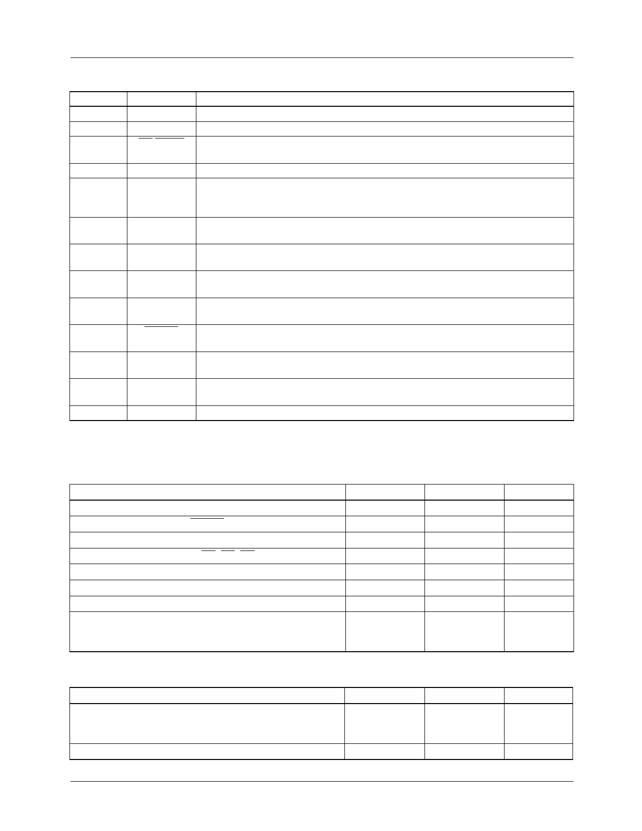
Pin Description (continued)
Pin
Name
Function
16
RVCO
An resistor to GND sets up a current proportional to the input voltage of the VCO.
17
C AT
A capacitor to GND sets the time that the controller stays in the align mode.
18
UV FAULT This output goes low when VDD drops below the UVLO threshold, and indicates that
all output drivers have been disabled.
19
C RT
A capacitor to GND sets the time that the controller stays in the ramp mode.
20
SPEED FB Output of the back-EMF sampling circuit and input to the VCO. An RC network
connected to SPEED FB sets the compensation for the PLL loop formed by the
back-EMF sampling circuit, the VCO, and the commutation state machine.
21
CRR
A capacitor to between CRR and SPEED FB sets the ramp rate (acceleration) of the
motor when the controller is in ramp mode.
22
FB A
The motor feedback voltage from phase A is monitored through a resistor divider for
back-EMF sensing at this pin.
23
FB B
The motor feedback voltage from phase B is monitored through a resistor divider for
back-EMF sensing at this pin.
24
FB C
The motor feedback voltage from phase C is monitored through a resistor divider for
back-EMF sensing at this pin.
25
BRAKE A logic low input activates motor braking by shutting off the high-side output drivers
and turning on the low-side output drivers.
26
CIOS
A capacitor to GND sets the time that the low-side output drivers remain off after
ISENSE exceeds its threshold .
27
RREF
An 137kΩ resistor to GND sets a current proportional to VREF that is used to set all
the internal bias currents except for the VCO.
28
GND
Signal and power ground.
Absolute Maximum Ratings
Absolute maximum ratings are those values beyond which the device could be permanently damaged. Absolute maximum
ratings are stress ratings only and functional device operation is not implied.
Parameter
VDD
Logic Inputs (SPEED FB, BRAKE)
All Other Inputs and Outputs
Output Current (LA, LB, LC, HA, HB, HC)
Junction Temperature
Storage Temperature Range
Lead Temperature (Soldering 10 sec.)
Thermal Resistance (θJA)
28-Pin Narrow PDIP
28-Pin SOIC
Min.
GND – 0.3
GND – 0.3
-65
Max.
14
7
VDD + 0.3
±50
150
150
260
48
75
Units
V
V
V
mA
°C
°C
°C
°C/W
°C/W
Operating Conditions
Parameter
Temperature Range
ML4425CX
ML4425IX
VDD
Min.
0
–40
10.8
Max.
70
85
13.2
Units
°C
°C
V
REV. 1.0.2 7/2/01
3
Share Link: 