ML3356 Ver la hoja de datos (PDF) - LANSDALE Semiconductor Inc.
Número de pieza
componentes Descripción
Fabricante
ML3356 Datasheet PDF : 9 Pages
| |||
ML3356
LANSDALE Semiconductor, Inc.
Legacy Applications Information
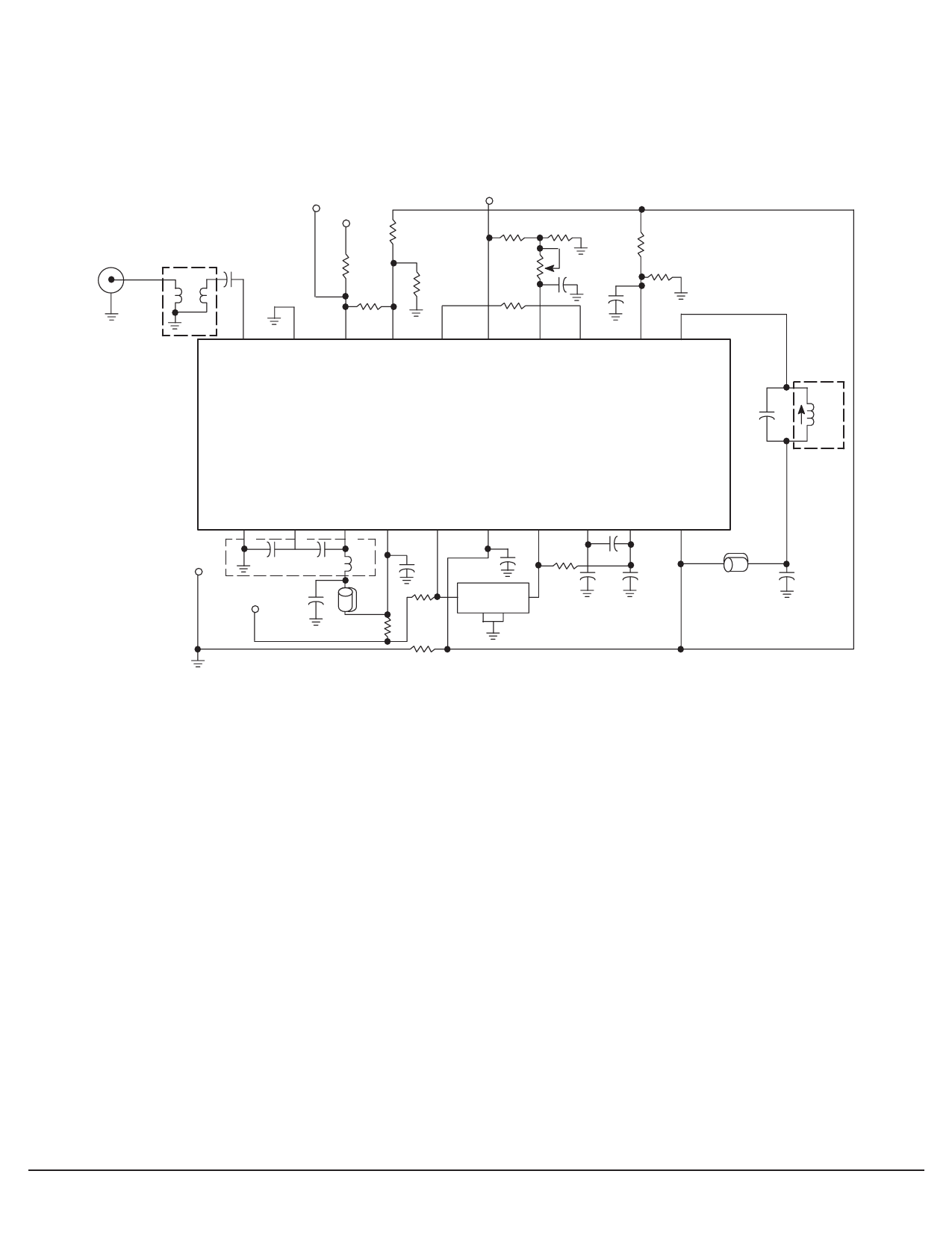
Figure 5. Application with Fixed Bias on Data Shaper
RF In
1:2
0.01
Data Out
5.0 V
18 k
Car. Det. Out
0 V or 4.0 V 3.3 k
130 k
15 k
10 k
10 k
390 k
3.0 k
3.3 k
0.1 470
pF
18 k
20
19
RF Input Ground
18
Data
Output
17
Comp(+)
16
15
Comp(–) Squelch
Status
14
13
Squelch Demod
Control Out
12
Demod
Filter
11
Quad
Input
ML3356
150 pF
RF
OSC
OSC RF
Mixer
Limiter Limiter Limiter Quad
Gnd
EM.
COL. VCC
Out
VCC
Input
Bias Bias
Bias
1
2
3
4
5
6
7
8
9
10
5.0 V
15 pF
5.6 pF fO
0.01
+ 5.0 to + 12 V 0.01
Bead
4.0 V
330
0.1
Cer. Fil.
10.7 MHz
330
0.01
0.01
0.01
Bead
0.1
180
82
APPLICATION NOTES (continued)
Shielding, which includes the placement of input and output
components, is important in minimizing electrostatic or elec-
tromagnetic coupling. The ML3356 has its pin connections
such that the circuit designer can place the critical input and
output circuits on opposite ends of the chip. Shielding is nor-
mally required for inductors in tuned circuits.
The ML3356 has a separate VCC and ground for the RF and
IF sections which allows good external circuit isolation by
minimizing common ground paths.
Note that the circuits of Figures 1 and 2 have RF, Oscillator,
and IF circuits predominantly referenced to the plus supply
rails. Figure 5, on the other hand, shows a suitable means of
ground referencing. The two methods produce identical results
when carefully executed. It is important to treat Pin 19 as a
ground node for either approach. The RF input should be
‘‘grounded’’ to Pin 1 and then the input and the mixer/oscilla-
tor grounds (or RF VCC bypasses) should be connected by a
low inductance path to Pin 19. IF and detector sections should
also have their bypasses returned by a separate path to Pin 19.
VCC and RF VCC can be decoupled to minimize feedback,
although the configuration of Figure 2 shows a successful
implementation on a common 5.0 V supply. Once again, the
message is: define a supply node and a ground node and return
each section to those nodes by separate, low impedance paths.
The test circuit of Figure 2 has a 3 dB limiting level of 30
µV which can be lowered 6 db by a 1:2 untuned transformer at
the input as shown in Figures 5 and 6. For applications that
require additional sensitivity, an RF amplifier can be added,
but with no greater than 20 db gain. This will give a 2.0 to 2.5
µV sensitivity and any additional gain will reduce receiver
dynamic range without improving its sensitivity. Although the
test circuit operates at 5.0 V, the mixer/oscillator optimum per-
formance is at 8.0 V to 12 V. A minimum of 8.0 V is recom-
mended in high frequency applications (above 150 MHz), or in
PLL applications where the oscillator drives a prescaler.
Page 4 of 9
www.lansdale.com
Issue A
Share Link: 