MH8V7245BAZTJ-6 Ver la hoja de datos (PDF) - MITSUBISHI ELECTRIC
Número de pieza
componentes Descripción
Fabricante
MH8V7245BAZTJ-6
MITSUBISHI ELECTRIC

MH8V7245BAZTJ-6 Datasheet PDF : 23 Pages
| |||
Preliminary Spec.
Specifications subject to
change without notice.
MITSUBISHI LSIs
MH8V7245BAZTJ -5, -6
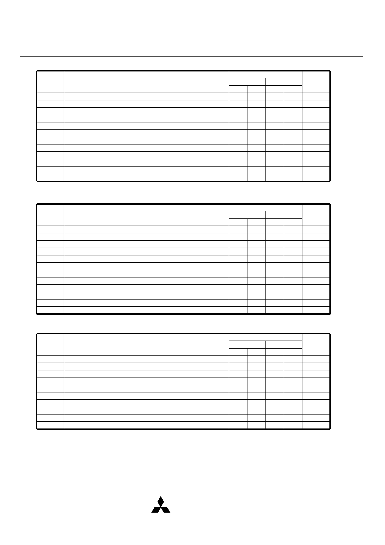
HYPER PAGE MODE 603979776 - BIT ( 8388608 - WORD BY 72 - BIT ) DYNAMIC RAM
Read and Refresh Cycles
Symbol
Parameter
tRC
Read cycle time
tRAS /RAS low pulse width
tCAS /CAS low pulse width
tCSH /CAS hold time after /RAS low
tRSH /RAS hold time after /CAS low
tRCS Read Setup time after /CAS high
tRCH Read hold time after /CAS low
tRRH Read hold time after /RAS low
tRAL Column address to /RAS hold time
tCAL Column address to /CAS hold time
tORH /RAS hold time after /OE low
tOCH /CAS hold time after /OE low
Note 22: Either tRCH or tRRH must be satisfied for a read cycle.
(Note 22)
(Note 22)
Limits
-5
-6
Unit
Min Max Min Max
84
104
ns
50 10000 60 10000
ns
8 10000 10 10000
ns
30
35
ns
18
20
ns
0
0
ns
0
0
ns
-5
-5
ns
30
35
ns
13
18
ns
18
20
ns
13
15
ns
Write Cycle (Early Write and Delayed Write)
Symbol
Parameter
tWC
tRAS
tCAS
tCSH
tRSH
tWCS
tWCH
tCWL
tRWL
tWP
tDS
tDH
Write cycle time
/RAS low pulse width
/CAS low pulse width
/CAS hold time after /RAS low
/RAS hold time after /CAS low
Write setup time before /CAS low
Write hold time after /CAS low
/CAS hold time after /W low
/RAS hold time after /W low
Write pulse width
Data setup time before /CAS low or /W low
Data hold time after /CAS low or /W low
(Note 24)
Limits
-5
-6
Unit
Min Max Min Max
84
104
ns
50 10000 60 10000 ns
8 10000 10 10000 ns
30
35
ns
18
20
ns
0
0
ns
8
10
ns
8
10
ns
13
15
ns
8
10
ns
-5
-5
ns
13
15
ns
Read-Write and Read-Modify-Write Cycles
Symbol
Parameter
tRWC
tRAS
tCAS
tCSH
tRSH
tRCS
tCWD
tRWD
tAWD
tOEH
Read write/read modify write cycle time
/RAS low pulse width
/CAS low pulse width
/CAS hold time after /RAS low
/RAS hold time after /CAS low
Read setup time before /CAS low
Delay time, /CAS low to /W low
Delay time, /RAS low to /W low
Delay time, address to /W low
/OE hold time after /W low
(Note23)
(Note24)
(Note24)
(Note24)
Limits
-5
-6
Unit
Min Max Min Max
109
133
ns
75 10000 89 10000 ns
38 10000 44 10000
ns
65
77
ns
43
49
ns
0
0
ns
28
32
ns
60
72
ns
40
47
ns
13
15
ns
Note 23: tRWC is specified as tRWC(min)=tRAC(max)+tODD(min)+tRWL(min)+tRP(min)+4tT.
24:tWCS, tCWD,tRWD ,tAWD and,tCPWD are specified as reference points only. If tWCS≥tWCS(min) the cycle is an early write cycle and the DQ pins will remain
high impedance throughout the entire cycle. If tCWD≥tCWD(min), tRWD≥tRWD (min), tAWD≥tAWD(min) and tCPWD ≥tCPWD(min) (for Hyper page mode cycle only),
the cycle is a read-modify-write cycle and the DQ will contain the data read from the selected address. If neither of the above condition (delayed write) of the DQ (at access
time and until /CAS or /OE goes back to VIH) is indeterminate.
MIT-DS-0284-0.0
MITSUBISHI
ELECTRIC
( 7 / 23 )
9/Nov. /1998
Share Link: