MB90352S Ver la hoja de datos (PDF) - Fujitsu
Número de pieza
componentes Descripción
Fabricante
MB90352S Datasheet PDF : 64 Pages
| |||
MB90350 Series
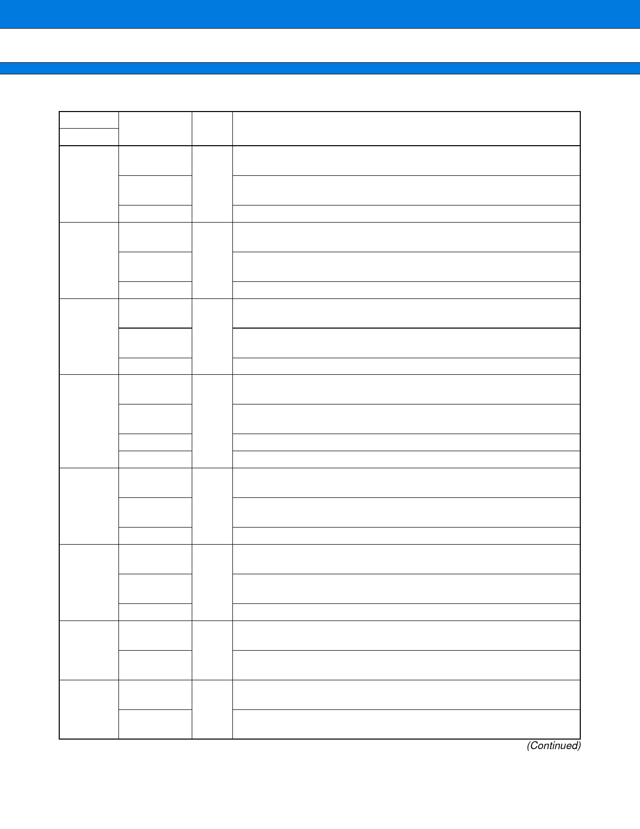
Pin No.
LQFP64*
24 to 31
32
33
34
35
36
37
38
Pin name
Circuit
type
Function
P00 to P07
General purpose I/O ports.The register can be set to select whether to use
a pull-up resistor.This function is enabled in single-chip mode.
AD00 to AD07
G
Input/output pins of external address data bus lower 8 bit. This function is
enabled when the external bus is enabled.
INT8 to INT15
External interrupt request input pins for INT8 to INT15.
P10
General purpose I/O port.The register can be set to select whether to use
a pull-up resistor.This function is enabled in single-chip mode.
AD08
G Input/output pin for external bus address data bus bit 8.
This function is enabled when external bus is enabled.
TIN1
Event input pin for reload timer1.
P11
General purpose I/O.The register can be set to select whether to use a
pull-up resistor.This function is enabled in single-chip mode.
AD09
G Input/output pin for external bus address data bus bit 9. This function is en-
abled when external bus is enabled.
TOT1
Output pin for reload timer1.
P12
General purpose I/O port. The register can be set to select whether to use
a pull-up resistor. This function is enabled in single-chip mode.
AD10
Input/output pin for external bus address data bus bit 10. This function is
N enabled when external bus is enabled.
SIN3
Serial data input pin for UART3.
INT11R
External interrupt request input pin for INT11
P13
General purpose I/O port. The register can be set to select whether to use
a pull-up resistor. This function is enabled in single-chip mode.
AD11
G Input/output pin for external bus address data bus bit 11.
This function is enabled when external bus is enabled.
SOT3
Serial data output pin for UART3.
P14
General purpose I/O port. The register can be set to select whether to use
a pull-up resistor. This function is enabled in single-chip mode.
AD12
G Input/output pin for external bus address data bus bit 12.
This function is enabled when external bus is enabled.
SCK3
Clock input/output pin for UART3.
P15
AD13
General purpose I/O port. The register can be set to select whether to use
a pull-up resistor. This function is enabled in single-chip mode.
N
Input/output pin for external bus address data bus bit 13.
This function is enabled when external bus is enabled.
P16
AD14
General purpose I/O port. The register can be set to select whether to use
a pull-up resistor. This function is enabled in single-chip mode.
G
Input/output pin for external bus address data bus bit 14.
This function is enabled when external bus is enabled.
(Continued)
8
Share Link: 