ICM7231 Ver la hoja de datos (PDF) - Intersil
Número de pieza
componentes Descripción
Fabricante
ICM7231 Datasheet PDF : 16 Pages
| |||
ICM7231, ICM7232
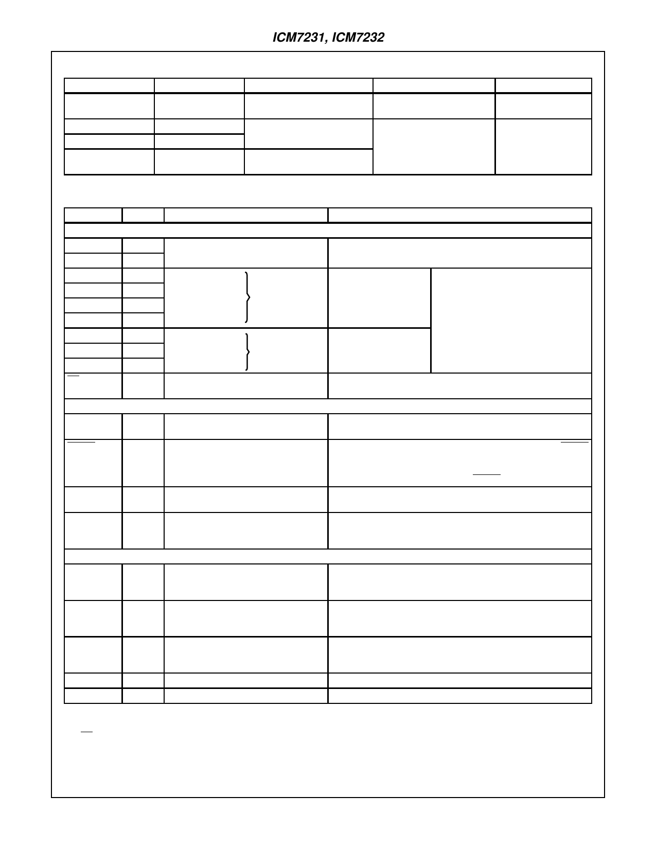
Table of Features
TYPE NUMBER
ICM7231BF
OUTPUT CODE
Code B
ICM7232AF
ICM7232BF
ICM7232CR
Hexadecimal
Code B
Code B
ANNUNCIATOR LOCATIONS
INPUT
OUTPUT
Both Annunciators on BP3
Parallel Entry, 4-bit Data, 2-bit 8 Digits plus
Annunciators, 3-bit Address 16 Annunciators
Both Annunciators on BP3
Serial Entry, 4-bit Data, 2-bit 10 Digits plus
Annunciators, 4-bit Address 20 Annunciators
1 Annunciator BP1
1 Annunciator BP3
Terminal Definitions
TERMINAL PIN NO.
DESCRIPTION
ICM7231 PARALLEL INPUT NUMERIC DISPLAY
AN1
30 Annunciator 1 Control Bit
High = ON
FUNCTION
AN2
31 Annunciator 2 Control Bit
Low = OFF
See Table 3
BD0
32 Least Significant
Input
HIGH = Logical One (1)
BD1
33
BD2
34
4-bit Binary
Data Inputs
Data
(See Table 1)
LOW = Logical Zero (0)
BD3
35 Most Significant
A0
37 Least Significant
Input
A1
38
3-bit Digit
Address Inputs
Address
(See Table 2)
A2
39 Most Significant
CS
1 Data Input Strobe/Chip Select (Note 2) Trailing (Positive going) edge latches data, causes data input to be
decoded and sent out to addressed digit
ICM7232 SERIAL DATA AND ADDRESS INPUT
Data Input
WRITE Input
38 Data+ Address Shift Register Input
39 Decode, Output, and Reset Strobe
HIGH = Logical One (1)
LOW = Logical Zero (O)
When DATA ACCEPTED Output is LOW, positive going edge of WRITE
causes data in shift register to be decoded and sent to addressed digit,
then shift register and control logic to be reset. When DATA ACCEPTED
Output is HIGH, positive going edge of WRITE triggers reset only.
Data Clock
Input
DATA
ACCEPTED
Output
1 Data Shift Register and Control Logic
Clock
37 Handshake Output
Positive going edge advances data in shift register. ICM7232: Elev-
enth edge resets shift register and control logic.
Output LOW when correct number of bits entered into shift register.
ALL DEVICES
Display
Voltage
VDlSP
Common
Line Driver
Outputs
Segment
Line Driver
Outputs
2
3, 4, 5
Negative end of on-chip resistor string Display voltage control. When open (or less than 1V from VDD) chip
used to generate intermediate voltage is shutdown; oscillator stops, all display pins to VDD.
levels for display. Shutdown Input.
Drive display commons, or rows
6 - 29 (On ICM7231)
6 - 35 (On ICM7232)
Drive display segments, or columns.
VDD
40 Chip Positive Supply
VSS
36 Chip Negative Supply
NOTES:
1. For Design reference only, not 100% tested.
2. CS has a special “mid-level” sense circuit that establishes a test mode if it is held near 3V for several ms. Inadvertent triggering of this
mode can be avoided by pulling it high when inactive, or ensuring frequent activity.
9-24
Share Link: 