M66220 Ver la hoja de datos (PDF) - Mitsumi
N√Їmero de pieza
componentes Descripción
Fabricante
M66220 Datasheet PDF : 11 Pages
| |||
MITSUBISHI вМ©DIGITAL ASSPвМ™
M66220SP/FP
256 √Ч 8-BIT MAIL-BOX
FUNCTION
The M66220 is a mail box most suitable for inter-MPU data transfer
which is used in a multiport mode. Provision of two pairs of addresses
and data buses in its shared memory cell of 256 √Ч 8 bit configuration
allows independent and asynchronous read/write operations from/to
two access ports of A and B individually.
This allows access to shared memory as simple RAM when viewing
from one MPU. The concurrent accessibility to shared memory from
two MPUs provides remarkable improvement of a multiport mode
processor system in throughput.
The arbitration function incorporated in the chip decides the first-in
port to assign a higher priority to the access from one MPU, even if
two MPUs contend for selection of the same address in shared
memory from ports A and B. A Not Ready signal вАЬLвАЭ is output to the
last-in port and invalidates any access from the other MPU.
As a write operation to memory, one of addresses A0 to A7 is specified.
The CS signal is set to вАЬLвАЭ to place one of I/O pins in the input mode.
Also, the WE signal is set to вАЬLвАЭ. Data at the I/O pin is thus written
into memory.
As a read operation, the WE signal is set to вАЬHвАЭ. Both CS signal and
OE signal are set to вАЬLвАЭ to place one of I/O pins in the output mode.
One of addresses A0 to A7 is specified. Data at the specified address
is output to the I/O pin.
When the CS signal is set to вАЬHвАЭ, the chip enters a non-select state
which inhibits a read and write operation. At this time, the output is
placed in the floating state (high impedance state), thus allowing OR
tie with another chip. When the OE signal is set to вАЬHвАЭ, the output
enters the floating state. In the I/O bus mode, setting the OE signal
to вАЬHвАЭ at a write time avoids contention of I/O bus data. When the CS
signal is set to Vcc, the output enters the full stand-by state to minimize
supply current (See Tables 1 and 2).
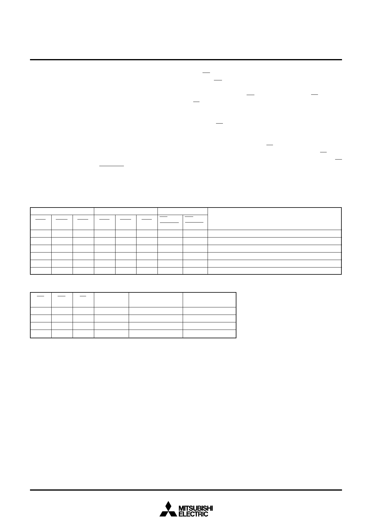
Table 1 Mode Settings of Ports (A0A ~ A7A вЙ† A0B ~ A7B)
A port input
B port input
Flag
CSA
WEA
OEA
CSB
WEB
OEB
Not
Not
Ready A Ready B
H
√Ч
√Ч
√Ч
√Ч
√Ч
H
H
√Ч
√Ч
√Ч
H
√Ч
√Ч
H
H
L
L
√Ч
√Ч
√Ч
√Ч
H
H
L
H
L
√Ч
√Ч
√Ч
H
H
√Ч
√Ч
√Ч
L
L
√Ч
H
H
√Ч
√Ч
√Ч
L
H
L
H
H
Operation
A port is set to the non-select mode.
B port is set to the non-select mode.
A port is set to the write mode for memory.
A port is set to the read mode for memory.
B port is set to the write mode for memory.
B port is set to the read mode for memory.
Table 2 Basic Functions of Ports
CS
WE
OE
Mode
H
√Ч
√Ч
Non-select
L
L
√Ч
Write
L
H
L
Read
L
H
H
Note 1: √Ч indicates вАЬLвАЭ or вАЬHвАЭ. (Irrelevant)
вАЬHвАЭ = High level, вАЬLвАЭ = Low level
I/O pin
High impedance
DIN
DOUT
High impedance
ICC
Stand-by
Operation
Operation
Operation
2
Share Link: 