M63001FP Ver la hoja de datos (PDF) - Mitsumi
Número de pieza
componentes Descripción
Fabricante
M63001FP Datasheet PDF : 10 Pages
| |||
MITSUBISHI SEMICONDUCTORS
M63001FP
6CH ACTUATOR DRIVER
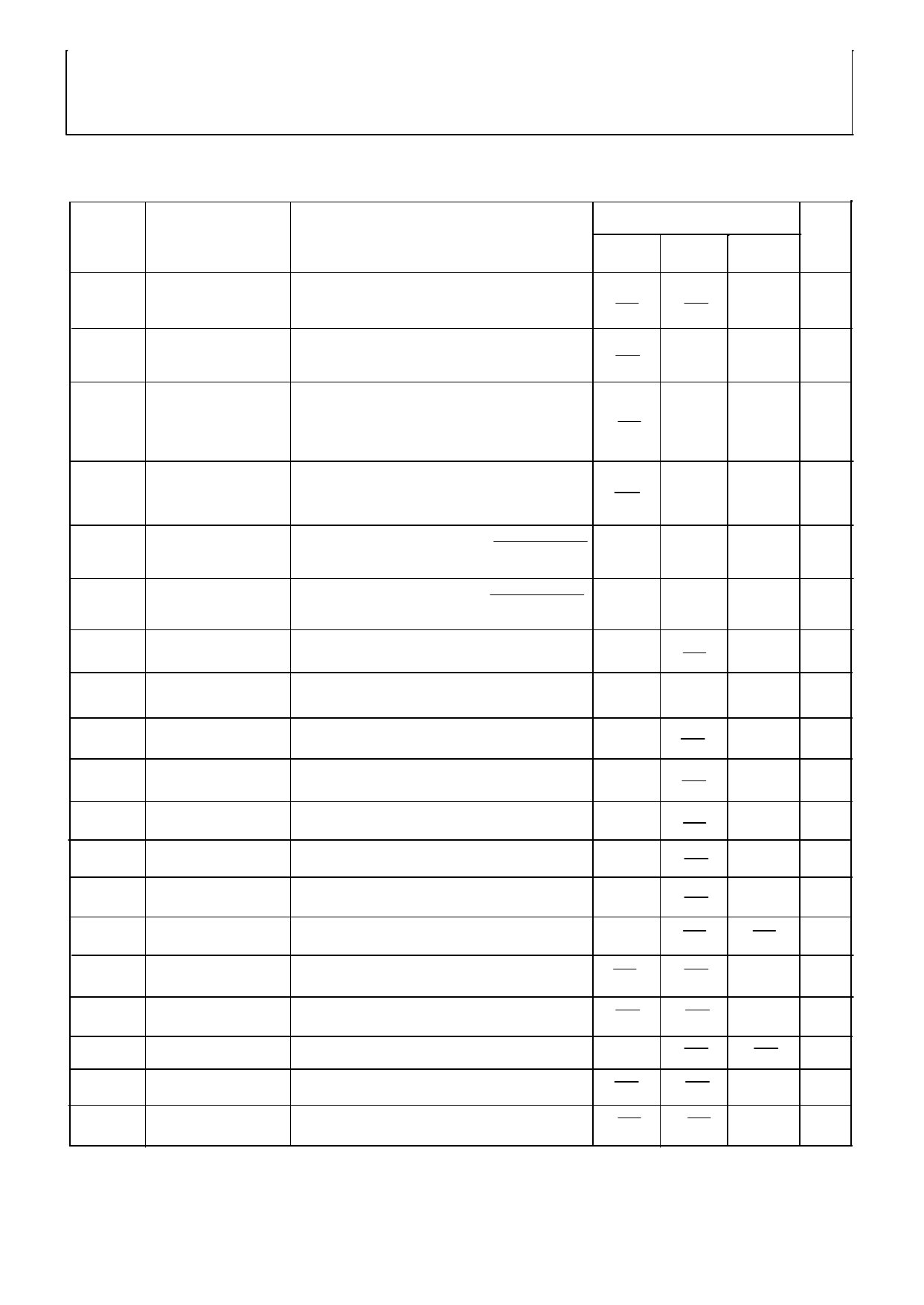
<ELECTRICAL CHARACTERISTICS>
SYMBOL PARAMETER
(Ta=25ºC, VCC1=VCC2=VCC3=VCC4=5V unless otherwise noted.)
CONDITIONS
LIMITS
MIN
TYP
MAX
Units
IccS
Icc
VCC1 and VCC2 and VCC3 and VCC4 total input current
STANDBY circuit current (STANDBY= Low or OPEN)
VCC1 and VCC2 and VCC3 and VCC4 total input current
Sleep Mode supply current(VREF=IN(+)=IN( -)=2.5V,IN1B(-)=Open,Standby= Hi)
10
uA
24
34
mA
Vsat1 Output Saturation voltage1
Top and Bottom saturation voltage.
(CH1,CH2,CH3,CH5,CH6)
Load current 0.3A(bootstrap)
1.5
2.1
V
Vsat2 Output Saturation voltage2
Top and Bottom saturation voltage.(CH4)
Load current 0.5A(bootstrap)
Gain1 Gain between input and
output 1
Gain2 Gain between input and
output 2
Vofs1
Output offset voltage 1
Vofs2 Output offset voltage 2
Vin1 Input voltage range1
OUT(-)-OUT(+)
CH1,CH2,CH3,CH4
Gain1=
Gain between input and output
IN(-)-VREF
CH5,CH6
OUT(-)-OUT(+)
Gain2=
IN(-)-IN(+)
Gain between input and output
7.60
7.04
Output offset voltage(CH1,CH2,CH3,CH4)
-35
IN(+)=VREF(2.5V)
Output offset voltage(CH5,CH6)
IN(+)=IN(-)=(2.5V)
-35
Input voltage range <CH1(IN1A-) and CH2,CH3(IN-)>
0
Vin2 Input voltage range2
Input voltage range <CH4(IN-)>
0
Vin3 Input voltage range3
Input voltage range <IN5-,IN5+)>
0
Vin4 Input voltage range4
Input voltage range <IN6-,IN6+)>
0
VinR VREF input voltage range VCC1=VCC2
0
VsH
STANDBY H voltage
Minimum H voltage ofSTANDBY
2.0
VsL
STANDBY L voltage
Maximum L voltage of STANDBY
IsH
STANDBY input current H STANDBY input current (STANDBY=5V)
VmH MUTE H voltage
Minimum H voltage ofMUTE
2.0
VmL MUTE L voltage
Maximum L voltage of MUTE
ImH
MUTE input current H
MUTE input current (MUTE=5V)
1.5
8.52
7.96
0
2.1
V
9.35
dB
8.79 dB
+35 mV
+35 mV
VCC1
V
VCC2 V
VCC3 V
VCC4 V
VCC1
V
V
0.8
V
520 uA
V
0.8
V
520 uA
( 4 / 10 )
REV9806027
Share Link: 