M62021 Ver la hoja de datos (PDF) - MITSUBISHI ELECTRIC
Número de pieza
componentes Descripción
Fabricante
M62021 Datasheet PDF : 9 Pages
| |||
MITSUBISHI<Dig.Ana.INTERFACE>
M62021L,P,FP
SYSTEM RESET IC WITH SWITCH FOR MEMORY BACK-UP
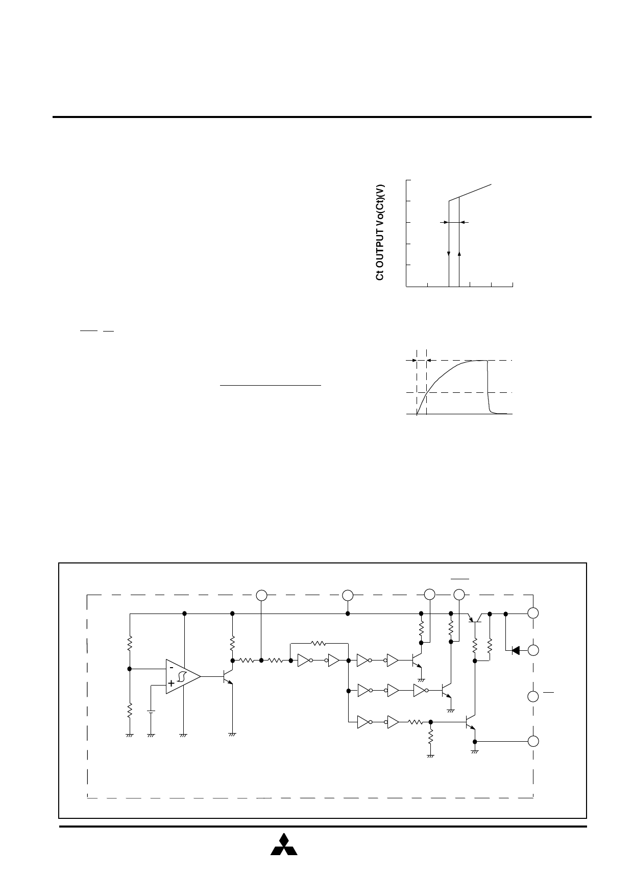
CONFIGURATION
<Power supply detector>
The internal reference voltage Vref is compared by means of
a comparator with resistor-divided voltage VR(resistor-divided
voltage produced by R1 and R2 from VIN).
If the input voltage is 5V,VR is set to 1.24V or higher,so the
comparator output is at low level and the Ct output(Q1
collector output)is set to high level.If the input voltage drops to
below 4.4V in an abnormal condition,VR becomes below
1.24V,so the comparator output goes from low to high level
and the Ct output,from high to low.The input voltage at this
point is called VSL.Next,when the input voltage,restored from
abnormal state,has a rise,the comparator output goes from
high to low level and the Ct output,from low to high.
The comparator used for detection has 100mV
hysteresis(∆Vs),so that malfunctioning is prevented in case
that the input voltage slowly drops or VR nearly equals Vref.
<Delay Circuit>
Connecting an external capacitor to the Ct pin lets
RES,RES,CS,and VOUT be delayed due to RC transient
phenomenon(electric charge).
Delay time is determined as follows.
5
4
3
∆Vs
2
VSL
VSH
1
0
4.0 4.2 4.4 4.6 4.8 5.0
INPUT VOLTAGE VIN(V)
tpd
VOH(Ct)
Delay time(tpd)= Ct X (R3 + R4) X In
=Ct X 22kΩ X 0.2614
.=.5.75 X 103 X Ct
[VOH(Ct)-VOL(Ct)]
[VOH(Ct)-INV1(VTH)]
*Ct is an external capacitance.
Taking into consideration the time taken by the oscillator of
microcomputer to be stable,connect a 4.7µF capacitor to the
Ct pin.
(As the response time of detection can be slowed due to
internal structure depending on the rising rate of power
supply,avoid connecting a too large capacitance.
<Schmitt trigger circuit>
Since waveforms show a gentle rise due to the RC delay
circuit,INV1,INV2,R5,and R6 constitute a schmitt trigger circuit
to produce hysteresis so as to prevent each output from
chattering.
INV1(Vth)
VOL(Ct)
DELAYED OUTPUT WAVEFORMS OF Ct
INTERNAL CIRCUIT
R1
60.94k
Com
R2
Vref
24K
1.24V
Ct
4
R3
22k
R4 R5
47 10k
Q1
VIN
RES RES
3
5
7
Q4
R7 R8
R6
10k 10k
R10
Q2
800
INV1 INV2 INV3 INV4
Q3
INV5 INV6 INV7
R9
INV8
INV9 5k
R10
22k
Q5
D1
R11
10k
1 VOUT
2 VBAT
8 CS
6 GND
MITSUBISHI
ELECTRIC
( 5 /9)
Share Link: 