M61500FP Ver la hoja de datos (PDF) - Renesas Electronics
Número de pieza
componentes Descripción
Fabricante
M61500FP Datasheet PDF : 13 Pages
| |||
M61500FP
Electrical Characteristics
(VDD = 2.5 V, VSS = –2.5 V, f = 1 kHz, Vi = 100 mV (rms), VOL = 0 dB, BASS = 0 dB, TREBLE = 0 dB,
VOL/TREBLE SHARE AMP = 18 dB, SURROUND = BYPASS, RL = 10 kΩ, Ta = 25°C, unless otherwise noted)
Item
Symbol Min
Typ
Max
Unit
Test Conditions
Circuit current of positive IDD
power supply
—
30
45
mA Quiescent
Circuit current of negative ISS
—
–30
–45
mA Quiescent
power supply
Voltage gain (selector)
Gv1
16
18
20
dB Vol/Treble share amp gain = 18 dB,
Bypass
Voltage gain (tone control) Gv2
25.5
27.5
29.5
dB Vol/Treble share amp gain = 18 dB,
QSurround mode, Vi = 20 mVrms
Maximum output voltage Vomax
1.2
1.6
—
Vrms RL = 10 kΩ, THD = 1%
Total harmonic distortion THD
—
0.02
0.08
% BW = 400 to 30 kHz
Output noise voltage
No1
—
6
15
μVrms JIS-A, Rg = 5.1 kΩ,
VOL = the infinitesimal, BYPASS
No2
—
11
30
μVrms JIS-A, Rg = 5.1 kΩ,
VOL = the infinitesimal,
QSurround mode
Maximum attenuation
ATTmax
—
–95
–90
dB Output reference level
(Vo = 1 Vrms),
ATT = the infinitesimal, JIS-A
Bass boost
GB1
GB2
1.5
3
4.5
dB 3 dB
f = 1 kHz,
4.5
6
7.5
6 dB
Vo = 80 mVrms
GB3
7.5
9
10.5
9 dB
GB4
10.5
12
13.5
12 dB
GB5
13.5
15
16.5
15 dB
GB6
16.5
18
19.5
18 dB
GB7
19.5
21
22.5
21 dB
Treble boost
GT1
1.5
3
4.5
GT2
4.5
6
7.5
3 dB
6 dB
f = 1 kHz,
Vo = 80 mVrms
GT3
7.5
9
10.5
9 dB
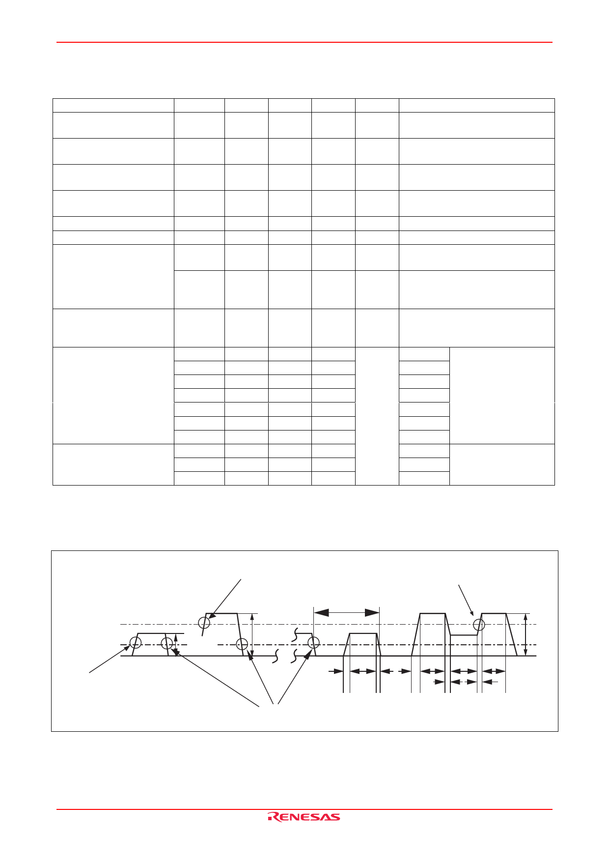
Control Signals Specification
(1) Waveform
Dn + 0
(CLOCK, H
DATA, M
STROBE) L
0 V DATA: L
Threshold of
the internal CLOCK.
Threshold of the internal
DATA (H/L)
Dn + 1
Dn + 10
Dn + 11
tcr
1.25 V
2.5 V
DATA: H
tWH
tr
tf
Threshold of the internal
STROBE.
tWH
tWL tWH
tr
tf
tr
The internal DATA latch at the falling edges of this clock signal.
2.5 V
REJ03F0274-0200 Rev.2.00 Jun 16, 2008
Page 5 of 12
Share Link: 