M5M5Y416CWG-70HI Ver la hoja de datos (PDF) - MITSUBISHI ELECTRIC
Número de pieza
componentes Descripción
Fabricante
M5M5Y416CWG-70HI Datasheet PDF : 10 Pages
| |||
2001.05.08 Ver. 3.0
MITSUBISHI LSIs
M5M5Y416CWG
-70HI, -85HI
Preliminary
Notice: This is not a final specification.
Some parametric limits are subject to change.
4194304-BIT (262144-WORD BY 16-BIT) CMOS STATIC RAM
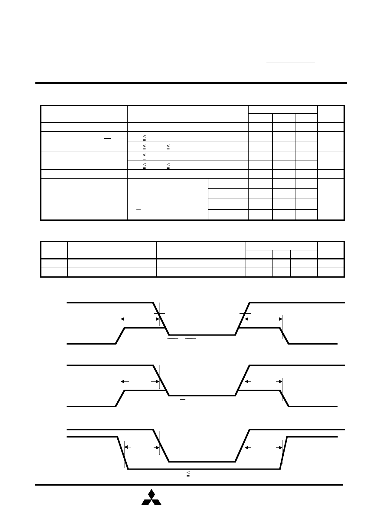
POWER DOWN CHARACTERISTICS
(1) ELECTRICAL CHARACTERISTICS
Symbol
Parameter
Test conditions
Vcc (PD) Power down supply voltage
VI (BC)
VI (S1)
Byte control input BC1 & BC2
Chip select input S1
1.65V Vcc(PD)
1.3V Vcc(PD) 1.65V
1.65V Vcc(PD)
1.3V Vcc(PD) 1.65V
VI (S2)
Chip select input S2
Icc (PD)
Power down
supply c urrent
Vcc=1.3V
(1) S1 => Vcc - 0.2V,
other inputs = 0 ~ Vcc
(2) S2 <= 0.2V,
other inputs = 0 ~ Vcc
(3) BC1 and BC2 =>Vcc - 0.2V
S1<= 0.2V, S2=> Vcc - 0.2V
other inputs = 0 ~ Vcc
(2) TIMING REQUIREMENTS
Limits
Min
Ty p Max Units
1.3
V
0.7xVcc
V
Vcc(PD)
0.7xVcc
V
Vcc(PD)
0.2
V
~ +25°C
-
0.1 0.7
~ +40°C
~ +70°C
-
0.2 1.5
µA
-
-
5
~ +85°C
-
-
10
Note 2: Typical parameter of Icc(PD) indicates the value for the
center of distribution at 1.3V, and not 100% tested.
Symbol
Parameter
tsu (PD)
trec (PD)
Power down set up time
Power down recov ery t ime
Test conditions
Limits
Min Ty p Max
0
5
Units
ns
ms
(3) TIMING DIAGRAM
BC control mode
Vcc
tsu (PD)
1.65V
1.65V
trec (PD)
0.7 x Vcc
BC1
BC2
S1 control mode
Vcc
tsu (PD)
BC1 , BC2>= Vcc-0.2V
1.65V
1.65V
trec (PD)
0.7 x Vcc
0.7 x Vcc
S1
S1 >= Vcc-0.2V
0.7 x Vcc
S2 control mode
Vcc
S2
0.2V
1.65V
tsu (PD)
1.65V
S2 0.2V
trec (PD)
0.2V
MITSUBISHI ELECTRIC
8
Share Link: 