M-8870-01 Ver la hoja de datos (PDF) - Unspecified
Número de pieza
componentes Descripción
Fabricante
M-8870-01 Datasheet PDF : 9 Pages
| |||
M-8870
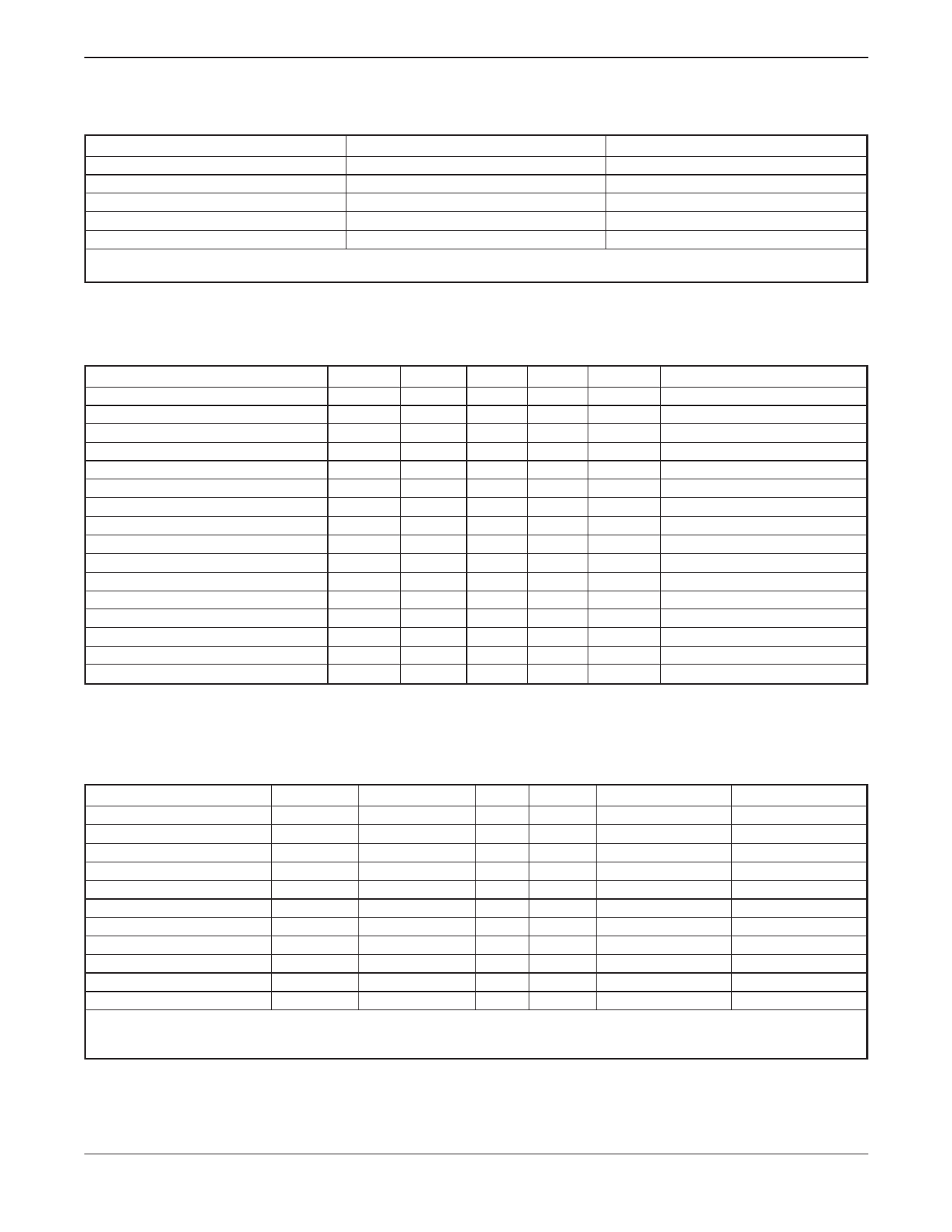
Table 2 Absolute Maximum Ratings
Parameter
Symbol
Value
Power supply voltage (VDD - VSS)
VDD
Voltage on any pin
VDC
Current on any pin
IDD
Operating temperature
TA
Storage temperature
TS
6.0 V max
VSS -0.3, VDD +0.3
10 mA max
-40°C to + 85°C
-65°C to + 150°C
Note:
Exceeding these ratings may cause permanent damage. Functional operation under these conditions is not implied.
Parameter
Operating supply voltage
Operating supply current
Standby supply current (see Note 3)
Power consumption
Low level input voltage
High level input voltage
Input leakage current
Pullup (source) current on OE
Input impedance, signal inputs 1, 2
Steering threshold voltage
Low level output voltage
High level output voltage
Output low (sink) current
Output high (source) current
Output voltage VREF
Output resistance VREF
Table 3 DC Characteristics
Symbol
VDD
IDD
IDDQ
PO
VIL
VIH
IIH/IIL
ISO
RIN
VTSt
VOL
VOH
IOL
IOH
VREF
ROR
Min
4.75
3.5
8
2.2
VDD - 0.03
1.0
0.4
2.4
Typ*
3.0
15
0.1
6.5
10
2.5
0.8
10
Max
5.25
7.0
100
35
1.5
15.0
2.5
0.03
2.7
Units
V
mA
µA
mW
V
V
µA
µA
mΩ
V
V
V
mA
mA
V
kΩ
Test Conditions
PD=VDD
f = 3.579 MHz, VDD = 5.0 V
VIN = VSS or VDD (see Note 2)
OE = 0 V
@ 1 kHz
No load
No load
VOUT = 0.4 V
VOUT = VDD - 0.4 V
No load
Table 4 Operating Characteristics - Gain Setting Amplifier
Parameter
Symbol
Min
Typ*
Max
Units
Input leakage current
IN
± 100
nA
Input resistance
RIN
4
MΩ
Input offset voltage
VOS
± 25
mV
Power supply rejection
PSRR
50
dB
Common mode rejection
CMRR
55
dB
DC open loop voltage gain
AVOL
60
dB
Open loop unity gain bandwidth
fC
1.2
1.5
MHz
Output voltage swing
VO
3.5
VP-P
Tolerable capacitive load (GS)
CL
100
pF
Tolerable resistive load (GS)
RL
50
kΩ
Common mode range
VCM
2.5
V P-P
*Typical figures are at 25°C and are for design aid only; not guaranteed and not subject to production testing.
Note:
1. All voltages referenced to VSS unless otherwise noted. For typical values VDD = 5.0 V, VSS = 0 V, TA = 25°C.
Test Conditions
VSS < VIN < VDD
1 KHz
-3.0V < VIN < 3.0V
RL ≥ 100 KΩ to VSS
No load
40-406-00011, Rev. F
Page 4
www.clare.com
Share Link: 