LW020A Ver la hoja de datos (PDF) - General Semiconductor
Número de pieza
componentes Descripción
Fabricante
LW020A Datasheet PDF : 16 Pages
| |||

LW020 Single-Output-Series Power Modules:
36 Vdc to 75 Vdc Inputs; 20 W
Data Sheet
April 2008
Characteristics Curves (continued)
Test Configurations
101%
VO, nom
100%
VO, nom
TO OSCILLOSCOPE
BATTERY
LTEST
12 µH
CS 220 µF
IMPEDANCE < 0.1 Ω
@ 20 ˚C, 100 kHz
CURRENT
PROBE
33 µF
VI(+)
VI(-)
50%
IO, max
25%
IO, max
TIME, t (100 µs/div)
8-1261(C).b
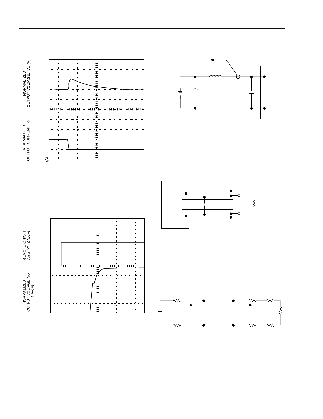
Figure 9. LW020A, B, C, F, and G Typical Output
Voltage for a Step Load Change from 50%
to 25%
8-203(C)
Note: Input reflected-ripple current is measured with a simulated
source impedance of 12 µH. Capacitor Cs offsets possible
battery impedance. Current is measured at the input of the
module.
Figure 11. Input Reflected-Ripple Test Setup
V O (+)
V O (-)
COPPER STRIP
0.1 µF SCOPE
RESISTIVE
LOAD
5V
0
100%
VO, nom
8-513(C)
Note: Use a 0.1 µF ceramic capacitor. Scope measurement should
be made using a BNC socket. Position the load between
50 mm and 75 mm (2 in. and 3 in.) from the module.
Figure 12. Peak-to-Peak Output Noise
Measurement Test Setup
50%
VO, nom
0
TIME, t (1 ms/div)
8-1263(C).b
Figure 10. LW020A, B, C, F, and G Typical Output
Voltage Start-Up when Signal Applied to
Remote On/Off
II
SUPPLY
VI(+) VO(+)
CONTACT AND
DISTRIBUTION LOSSES
IO
LOAD
CONTACT RESISTANCE
VI(-) VO(-)
8-204(C)
Note: All measurements are taken at the module terminals. When
socketing, place Kelvin connections at module terminals to
avoid measurement errors due to socket contact resistance.
η
=
⎛
⎝
[---V--[--O-V---(-I-+-(-+--)-)--–--–---V-V---O--I-(-(-–-–--)--)]--]I--II--O---⎠⎞
× 100
%
Figure 13. Output Voltage and Efficiency
Measurement Test Setup
8
Lineage Power