LTC1261I Ver la hoja de datos (PDF) - Linear Technology
Número de pieza
componentes Descripción
Fabricante
LTC1261I Datasheet PDF : 18 Pages
| |||
LTC1261
APPLICATIONS INFORMATION
OUTPUT RIPPLE
Output ripple in the LTC1261 comes from two sources;
voltage droop at the output capacitor between clocks and
frequency response of the regulation loop. Voltage droop
is easy to calculate. With a typical clock frequency of
550kHz, the charge on the output capacitor is refreshed
once every 1.8µs. With a 15mA load and a 3.3µF output
capacitor, the output will droop by:
ILOAD
•
∆t
COUT
=
15mA
•
1.8µs
3.3µF
=
8.2mV
This can be a significant ripple component when the output
is heavily loaded, especially if the output capacitor is small.
If absolute minimum output ripple is required, a 10µF or
greater output capacitor should be used.
Regulation loop frequency response is the other major
contributor to output ripple. The LTC1261 regulates the
output voltage by limiting the amount of charge transferred
to the output capacitor on a cycle-by-cycle basis. The
output voltage is sensed at the ADJ pin (COMP for fixed
output versions) through an internal or external resistor
divider from the OUT pin to ground. As the flying capaci-
tors are first connected to the output, the output voltage
begins to change quite rapidly. As soon as it exceeds the
set point COMP1 trips, switching the state of the charge
pump and stopping the charge transfer. Because the RC
time constant of the capacitors and the switches is quite
short, the ADJ pin must have a wide AC bandwidth to be
able to respond to the output in time. External parasitic
capacitance at the ADJ pin can reduce the bandwidth to
the point where the comparator cannot respond by the
time the clock pulse finishes. When this happens the
comparator will allow a few complete pulses through, then
overcorrect and disable the charge pump until the output
drops below the set point. Under these conditions the
output will remain in regulation but the output ripple will
increase as the comparator “hunts” for the correct value.
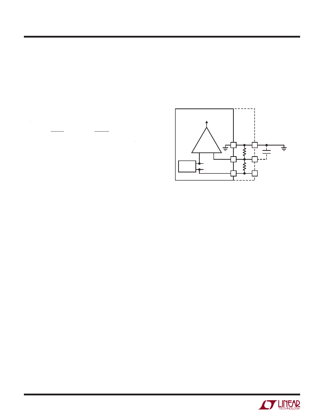
To prevent this from happening, an external capacitor
can be connected from ADJ (or COMP for fixed output
parts) to ground to compensate for external parasitics and
increase the regulation loop bandwidth (Figure 3). This
sounds coutnterintuitive until we remember that the internal
reference is generated with respect to OUT, not ground.
TO CHARGE
PUMP
RESISTORS ARE
INTERNAL FOR
FIXED OUTPUT PARTS
COMP 1
+
REF
– 1.24V
R1
CC
100pF
ADJ/COMP
R2
VOUT
LTC1261 • F03
Figure 3. Regulator Loop Compensation
The feedback loop actually sees ground as its “output,” thus
the compensation capacitor should be connected across
the “top” of the resistor divider, from ADJ (or COMP) to
ground. By the same token, avoid adding capacitance
between ADJ (or COMP) and VOUT. This will slow down
the feedback loop and increase output ripple. A 100pF
capacitor from ADJ or COMP to ground will compensate
the loop properly under most conditions.
OUTPUT FILTERING
If extremely low output ripple (< 5mV) is required, addi-
tional output filtering is required. Because the LTC1261
uses a high 550kHz switching frequency, fairly low value
RC or LC networks can be used at the output to effectively
filter the output ripple. A 10Ω series output resistor and
a 3.3µF capacitor will cut output ripple to below 3mV
(Figure 4). Further reductions can be obtained with larger
filter capacitors or by using an LC output filter.
1261fb
8
For more information www.linear.com/LTC1261
Share Link: 