LTC1261(RevA) Ver la hoja de datos (PDF) - Linear Technology
Número de pieza
componentes Descripción
Fabricante
LTC1261 Datasheet PDF : 16 Pages
| |||
LTC1261
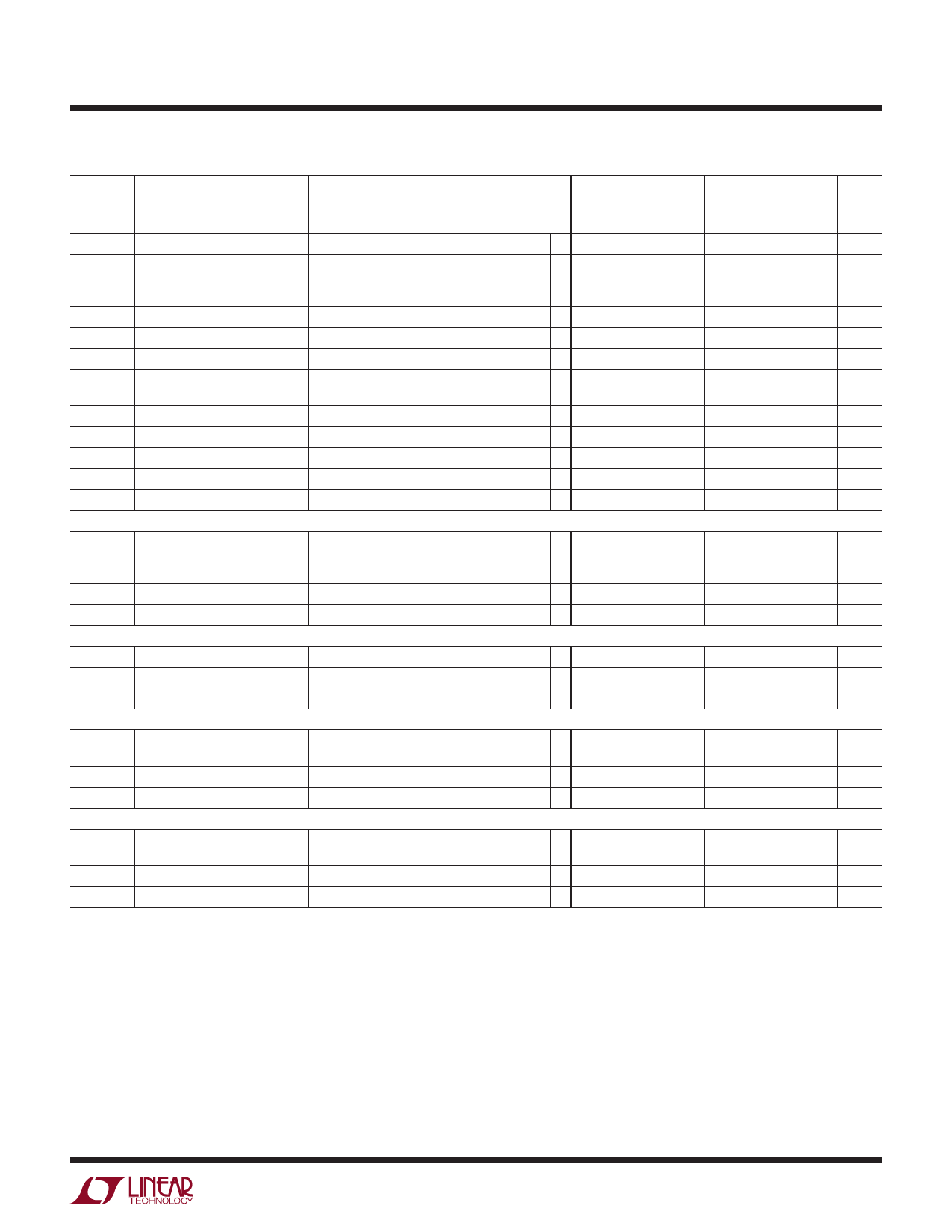
ELECTRICAL CHARACTERISTICS
Doubler Mode. VCC = 5V ±10%, C1 = 0.1µF, C2 = 0 (Note 4), COUT = 3.3µF unless otherwise specified.
0°C ≤ TA ≤ 70°C
SYMBOL PARAMETER
CONDITIONS (Note 2)
MIN TYP MAX
∆VOUT
ISC
VRIP
Output Regulation
(Note 2)
– 1.24V ≥ VOUT ≥ – 4V, 0 ≤ IOUT ≤ 8mA
q
– 1.24V ≥ VOUT ≥ – 4V, 0 ≤ IOUT ≤ 7mA
q
– 4V ≥ VOUT ≥ – 5V, 0 ≤ IOUT ≤ 8mA (Note 6)
Output Short-Circuit Current VOUT = 0V
q
Output Ripple Voltage
IOUT = 5mA, VOUT = – 4V
1
5
2
60 125
5
– 40°C ≤ TA ≤ 85°C
(Note 7)
MIN TYP MAX
1
5
2
60 125
5
UNITS
%
%
%
mA
mV
LTC1261CS Only. Tripler Mode. VCC = 2.7V, C1 = C2 = 0.1µF (Note 4), COUT = 3.3µF unless otherwise specified.
SYMBOL PARAMETER
CONDITIONS (Note 2)
0°C ≤ TA ≤ 70°C
MIN TYP MAX
– 40°C ≤ TA ≤ 85°C
(Note 7)
MIN TYP MAX
∆VOUT Output Regulation
– 1.24V ≥ VOUT ≥ – 4V, 0 ≤ IOUT ≤ 5mA
q
1
5
1
5
ISC
Output Short-Circuit Current VOUT = 0V
VRIP
Output Ripple Voltage
IOUT = 5mA, VOUT = – 4V
q
60 125
60 125
5
5
UNITS
%
mA
mV
LTC1261CS Only. Tripler Mode. VCC = 3.3V ±10%, C1 = C2 = 0.1µF (Note 4), COUT = 3.3µF unless otherwise specified.
SYMBOL PARAMETER
CONDITIONS (Note 2)
0°C ≤ TA ≤ 70°C
MIN TYP MAX
– 40°C ≤ TA ≤ 85°C
(Note 7)
MIN TYP MAX
∆VOUT Output Regulation
(Note 2)
– 1.24V ≥ VOUT ≥ – 4.5V, 0 ≤ IOUT ≤ 6mA
q
– 4.5V ≥ VOUT ≥ – 5V, 0 ≤ IOUT ≤ 3.5mA
q
ISC
Output Short-Circuit Current VOUT = 0V
q
VRIP
Output Ripple Voltage
IOUT = 5mA, VOUT = – 4V
1
5
2
5
35 75
5
1
5
2
35 75
5
UNITS
%
%
mA
mV
LTC1261CS Only. Tripler Mode. VCC = 5V ±10%, C1 = C2 = 0.1µF (Note 4), COUT = 3.3µF unless otherwise specified.
SYMBOL PARAMETER
∆VOUT Output Regulation
ISC
Output Short-Circuit Current
VRIP
Output Ripple Voltage
CONDITIONS (Note 2)
– 1.24V ≥ VOUT ≥ – 4V, 0 ≤ IOUT ≤ 12mA
– 4V ≥ VOUT ≥ – 5V, 0 ≤ IOUT ≤ 10mA
VOUT = 0V
IOUT = 5mA, VOUT = – 4V
0°C ≤ TA ≤ 70°C
MIN TYP MAX
– 40°C ≤ TA ≤ 85°C
(Note 7)
MIN TYP MAX UNITS
q
1
5
q
2
5
1
5
%
2
5
%
q
35 75
35 75
mA
5
5
mV
The q denotes specifications which apply over the full operating
temperature range.
Note 1: The Absolute Maximum Ratings are those values beyond which
the life of a device may be impaired.
Note 2: All currents into device pins are positive; all currents out of device
pins are negative. All voltages are referenced to ground unless otherwise
specified.
Note 3: All typicals are given at TA = 25°C.
Note 4: C1 = C2 = 0.1µF means the specifications apply to tripler mode
where VCC – VOUT = 3VCC (LTC1261CS only; the LTC1261CS8 cannot be
connected in tripler mode) with C1 connected between C1+ and C1 – and
C2 connected between C2 + and C2 –. C2 = 0 implies doubler mode where
VCC – VOUT = 2VCC; for the LTC1261CS this means C1 connects from C1+
to C2 – with C1 – and C2 + floating. For the LTC1261CS8 in doubler mode,
C1 connects from C1+ to C1 –; there are no C2 pins.
Note 5: Setting output to < – 7V will exceed the absolute voltage maximum
rating with a 5V supply. With supplies higher than 5V, the output should
never be set to exceed VCC – 12V.
Note 6: For output voltages below – 4.5V the LTC1261 may reach 50%
duty cycle and fall out of regulation with heavy load or low input voltages.
Beyond this point, the output will follow the input with no regulation.
Note 7: C grade device specifications are guaranteed over the 0°C to 70°C
temperature range. In addition, C grade device specifications are assured
over the –40°C to 85°C temperature range by design or correlation, but
are not production tested.
3
Share Link: 