LT3466 Ver la hoja de datos (PDF) - Linear Technology
Número de pieza
componentes Descripción
Fabricante
LT3466 Datasheet PDF : 20 Pages
| |||
LT3466
U
OPERATIO
Main Control Loop
The LT3466 uses a constant frequency, current mode
control scheme to provide excellent line and load regula-
tion. It incorporates two identical, but fully independent
PWM converters. Operation can be best understood by
referring to the Block Diagram in Figure 2. The oscillator,
start-up bias and the bandgap reference are shared be-
tween the two converters. The control circuitry, power
switch, Schottky diode etc., are all identical for both the
converters.
At power-up, the output voltages VOUT1 and VOUT2 are
charged up to VIN (input supply voltage) via their respec-
tive inductor and the internal Schottky diode. If either
CTRL1 and CTRL2 or both are pulled high, the bandgap
reference, start-up bias and the oscillator are turned on.
Working of the main control loop can be understood by
following the operation of converter 1. At the start of each
oscillator cycle, the power switch Q1 is turned on. A
voltage proportional to the switch current is added to a
stabilizing ramp and the resulting sum is fed into the
positive terminal of the PWM comparator A2. When this
voltage exceeds the level at the negative input of A2, the
PWM logic turns off the power switch. The level at the
negative input of A2 is set by the error amplifier A1, and is
simply an amplified version of the difference between the
feedback voltage and the 200mV reference voltage. In this
manner, the error amplifier A1 regulates the feedback
voltage to 200mV reference voltage. The output of the
error amplifier A1 sets the correct peak current level in
inductor L1 to keep the output in regulation. The CTRL1
pin voltage is used to adjust the reference voltage.
If only one of the converters is turned on, the other con-
verter will stay off and its output will remain charged up to
VIN (input supply voltage). The LT3466 enters into shut-
down, when both CTRL1 and CTRL2 are pulled lower than
50mV. The CTRL1 and CTRL2 pins perform independent
dimming and shutdown control for the two converters.
Minimum Output Current
The LT3466 can drive an 8-LED string at 2.5mA LED
current without pulse skipping. As current is further
reduced, the device may begin skipping pulses. This will
result in some low frequency ripple, although the LED
current remains regulated on an average basis down to
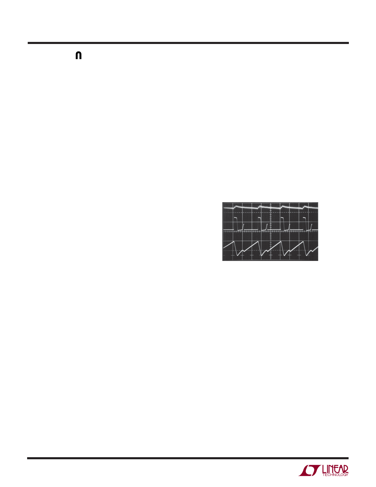
zero. The photo in Figure 3 shows circuit operation with 16
white LEDs (eight per converter) at 2.5mA current driven
from 3.6V supply. Peak inductor current is less than 50mA
and the regulator operates in discontinuous mode imply-
ing that the inductor current reached zero during the
discharge phase. After the inductor current reaches zero,
the switch pin exhibits ringing due to the LC tank circuit
formed by the inductor in combination with switch and
diode capacitance. This ringing is not harmful; far less
spectral energy is contained in the ringing than in the
switch transitions. The ringing can be damped by applica-
tion of a 300Ω resistor across the inductors, although this
will degrade efficiency.
VOUT1
10mV/DIV
VSW1
20V/DIV
IL1
50mA/DIV
VIN = 3.6V
0.5µs/DIV
ILED1 = 2.5mA
CIRCUIT OF FIGURE 1
3466 F03
Figure 3. Switching Waveforms
Open-Circuit Protection
The LT3466 has internal open-circuit protection for both
the converters. When the LEDs are disconnected from the
circuit or fail open, the converter output voltage is clamped
at 39.5V (typ). Figure 4a shows the transient response of
Figure 1’s step-up converter with LED1 disconnected.
With LED1 disconnected, the converter starts switching at
the peak inductor current limit. The converter output starts
ramping up and finally gets clamped at 39.5V (typ). The
converter will then switch at low inductor current to
regulate the converter output at the clamp voltage. Output
voltage and input current during output open circuit are
shown in the Typical Performance Characteristics graphs.
In the event one of the converters has an output open-
circuit, its output voltage will be clamped at 39.5V.
3466fa
8
Share Link: 