LT1118CS8-2.5 Ver la hoja de datos (PDF) - Linear Technology
Número de pieza
componentes Descripción
Fabricante
LT1118CS8-2.5
Linear Technology

LT1118CS8-2.5 Datasheet PDF : 8 Pages
| |||
LT1118/LT1118-2.5
LT1118-2.85/LT1118-5
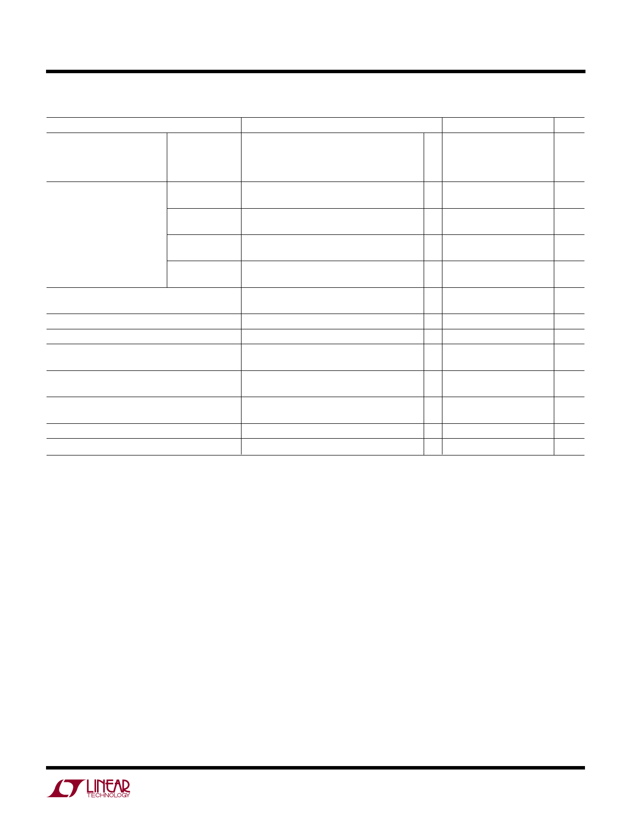
ELECTRICAL CHARACTERISTICS
The ● denotes specifications which apply over the full operating temperature range, otherwise specifications are at TA = 25°C. (Note 2)
PARAMETER
CONDITIONS
MIN TYP MAX UNITS
Line Regulation (Note 4)
LT1118
IL = 0mA, 4.2V ≤ VIN ≤ 15V
●
LT1118-2.5
IL = 0mA, 4.2V ≤ VIN ≤ 15V
●
LT1118-2.85
IL = 0mA, 4.75V ≤ VIN ≤ 15V
●
LT1118-5
IL = 0mA, 6.5V ≤ VIN ≤ 15V
●
6
mV
6
mV
6
mV
10
mV
Load Regulation (Note 4)
LT1118
0mA ≤ IL ≤ 800mA
– 400mA ≤ IL ≤ 0mA
●
6
mV
●
6
mV
LT1118-2.5
0mA ≤ IL ≤ 800mA
– 400mA ≤ IL ≤ 0mA
●
12
mV
●
12
mV
LT1118-2.85
LT1118-5
0mA ≤ IL ≤ 800mA
– 400mA ≤ IL ≤ 0mA
0mA ≤ IL ≤ 800mA
– 400mA ≤ IL ≤ 0mA
●
12
mV
●
12
mV
●
25
mV
●
25
mV
Dropout Voltage (Note 5)
IL = 100mA
IL = 800mA
0.85 1.1
V
1
1.3
V
FB Pin Bias Current
LT1118
0.35
1
µA
Minimum Output Voltage
LT1118
●
2.1
V
Ripple Rejection
Load Transient Settling Time,
∆V = 1%
Output Short-Circuit Current
ISC+
ISC–
fRIPPLE = 120Hz, VIN – VOUT = 2V
VRIPPLE = 0.5VP-P
0mA ≤ IL ≤ 800mA, CLOAD = 1µF
– 400mA ≤ IL ≤ 0mA, CLOAD = 1µF
VOUT = 0V
VOUT = VIN
60
80
dB
5
µs
5
µs
800 1200
mA
– 700 – 400
mA
Thermal Shutdown Junction Temperature
No Load
170
°C
Enable Turn-On Delay
No Load
50
µs
Note 1: Stresses beyond those listed under Absolute Maximum Ratings
may cause permanent damage to the device. Exposure to any Absolute
Maximum Rating condition for extended periods may affect device
reliability and lifetime.
Note 2: Unless otherwide specified, testing done at VCC = 5V
(LT1118-2.5, LT1118-2.85) or VCC = 7V (LT1118-5). VEN = VCC. Output
CLOAD = 1µF, ILOAD = 0.
Note 3: All operating conditions include the combined effects of load
current, input voltage and temperature over each parameter’s full range.
Note 4: Load and line regulation are tested at a constant junction
temperature by low duty cycle pulse testing.
Note 5: Dropout voltage is defined as the minimum input to output voltage
measured while sourcing the specified current.
1118fc
3
Share Link: