7083A1K Ver la hoja de datos (PDF) - Fairchild Semiconductor
Número de pieza
componentes Descripción
Fabricante
7083A1K Datasheet PDF : 16 Pages
| |||
ILC7083/ILC7084
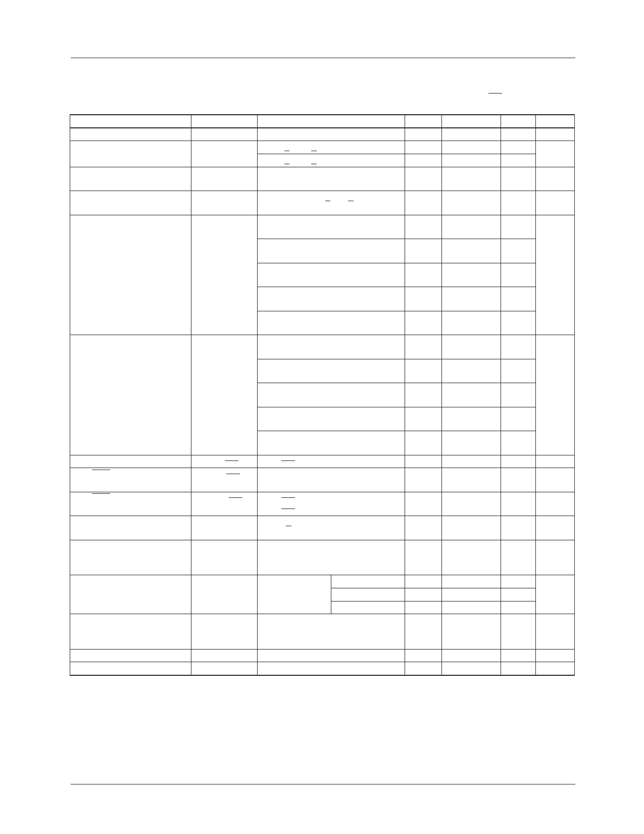
Electrical Characteristics ILC7083/ILC7084
Unless otherwise specified, all limits are at TA=25°C; VIN = VOUT(NOM) +1V, IOUT = 1mA, COUT = 1µF, VON/OFF = 2V.
Boldface type denotes specifications which apply over the specified operating temperature range.
Parameter
Symbol
Conditions
Min
Typ
Max Units
Input Voltage Range
Output Voltage
Feedback Voltage
(ADJ version)
VIN
VOUT
VADJ
1mA < IOUT < 150mA
1mA < IOUT < 150mA
2
-3
-4
1.217
1.204
VOUT(NOM)
VOUT(NOM)
1.255
13
+3
+4
1.292
1.305
V
%VOUT
(NOM)
V
Line Regulation
Dropout Voltage
(Note 3)
∆VOUT/
(VOUT*∆VIN)
VIN – VOUT
VOUT(NOM) +1V < VIN < 12V
IOUT= 0mA (Note 4)
0.007
0.1
0.014 %/V
0.032
1
mV
2
IOUT = 10mA
10
25
35
IOUT = 50mA
50
75
100
IOUT = 100mA
100
150
200
IOUT = 150mA
150
225
300
Ground Pin Current
IGND
IOUT = 0mA
95
200
µA
220
IOUT = 10mA
100
220
240
IOUT = 50mA
100
220
240
IOUT = 100mA
100
240
260
IOUT = 150mA
115
260
280
Shutdown (OFF) Current
ON/OFF Input Voltage
ION/OFF
VON/OFF
VON/OFF = 0V
High = Regulator On
Low = Regulator Off
0.1
2
µA
1.5
0.6
ON/OFF Pin Input
Current
IIN( ON/OFF)
VON/OFF = 0.6V, regulator OFF
VON/OFF = 2V, regulator ON
0.3
µA
1
Peak Output Current
IOUT(peak)
VOUT > 0.95VOUT(NOM),
400
500
mA
(Note 4)
tpw = 2ms
Output Noise Voltage (RMS)
eN
Ripple Rejection
∆VOUT/∆VIN
BW = 300Hz to 50kHz, CIN = 1µF
CNOISE = 0.01µF, COUT = 2.2µF,
IOUT = 10mA
COUT = 4.7µF,
IOUT = 100mA
Freq. = 1kHz
Freq. = 10kHz
40
µVRMS
85
dB
70
Freq. = 1MHz
60
Dynamic Line Regulation
Dynamic Load Regulation
Short Circuit Current
∆VOUT(line)
∆VOUT(load)
ISC
VIN: VOUT(NOM) + 1V to
VOUT(NOM) + 2V,
tr/tf = 2µs; IOUT = 150mA
IOUT: 1mA to 150mA; tr < 5µS
VOUT = 0V
14
mV
40
mV
600
mA
Notes:
1. Absolute maximum ratings indicate limits which when exceeded may result in damage to the component. Electrical specifications do not apply
when operating the device outside of its rated operating conditions.
2. Specified Min/Max limits are production tested or guaranteed through correlation based on statistical control methods.
Measurements are taken at constant junction temperature as close to ambient as possible using low duty pulse testing.
3. Dropout voltage is defined as the input to output differential voltage at which the output voltage drops 2% below the nominal value measured
with an IV differential.
4. Guaranteed by design.
4
REV. 1.0.9 1/28/03
Share Link: 