NJM2211D Ver la hoja de datos (PDF) - Japan Radio Corporation
Número de pieza
componentes Descripción
Fabricante
NJM2211D Datasheet PDF : 10 Pages
| |||
NJM2211
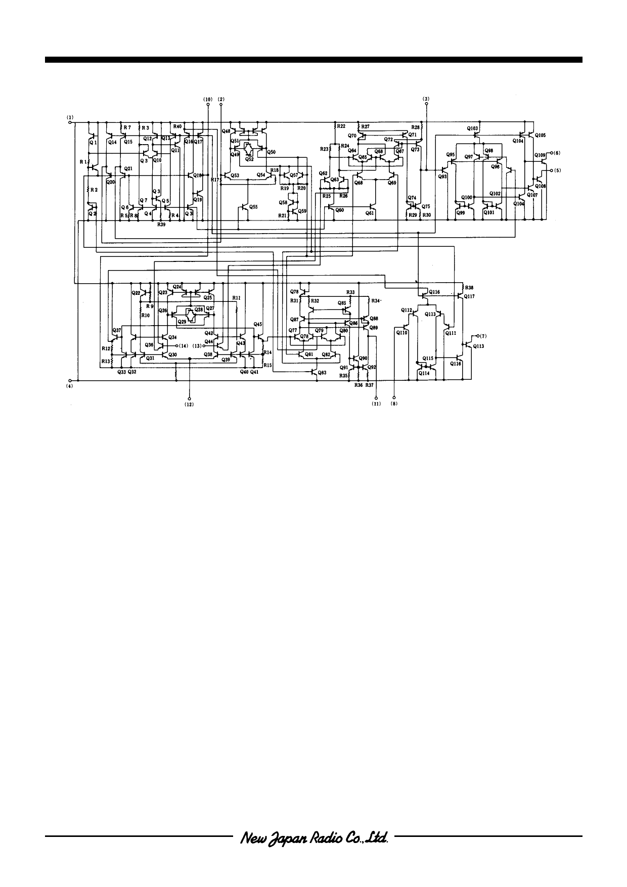
■ EQUIVALENT CIRCUIT
■ CIRCUIT FUNCTION
● Signal Input (Pin 2)
The input signal is AC coupled to this terminal. The internal impedance at pin 2 is 20kΩ, Recommended input signal
leveles in the range of 10mVrms to 3Vrms.
● Quadrature Phase Detector Output (Pin 3)
This is the high-impedance output of the quadrature phase detector, and is internally connected to the input of lock-detect
voltage comparator. In tone detection applications, pin 3 is connected to ground through a parallel combination of RD and
CD (see Figure 1) to eliminate chatter at the lock-detect outputs. If this tone-detect section is not used, pin 3 can be left
open circuited.
● Lock-Detect Output, Q (Pin 5)
The output at pin 5 is at a "high" state when the PLL is out of lock and goes to a "low" or conducting state when the PLL is
locked. It is an open collector type output and required a pull-up resistor, RL, to V+ for proper operation. In the "low" state it
can sink up to 5mA of load current.
● Lock-Detect Complement, Q (Pin 6)
The output at pin 6 is the logic complement of the lock-detect output at pin 5. This output is also an open collector type
stage which can sink 5mA of load current in the low or "on" state.
● FSK Data Output (Pin 7)
This output is an open collector logic stage which requres a pull-up resistor, RL, to V+ for proper operation. It can sink 5mA
of load current. When decoding FSK signals the FSK data output will switch to a "high"or off state for low input frequency,
and will switch to a "low" or on state for high input frequency. If no input signal is present, the logic state at pin 7 is
indeterminate.
● FSK Comparator Input (Pin 8)
This is the high-impedance input to the FSK voltage comparator. Normally, an FSK post-detection or data filter is
connected between this terminal and the PLL phase-detector output (pin 11). This data filter is formed by RF and CF of
Figure 1. The threshold voltage of the comparator is set by the internal reference voltage, VR, available at pin 10.
-4-
Ver.2003-12-09
Share Link: 