UPC8172TB(2001) Ver la hoja de datos (PDF) - NEC => Renesas Technology
Número de pieza
componentes Descripción
Fabricante
UPC8172TB
(Rev.:2001)
(Rev.:2001)
NEC => Renesas Technology

UPC8172TB Datasheet PDF : 8 Pages
| |||
UPC8187TB
ABSOLUTE MAXIMUM RATINGS1
(TA = +25°C unless otherwise specified)
SYMBOLS
PARAMETERS
UNITS RATINGS
VCC
Supply Voltage
PD
Power Dissipation2
V
3.6
mW
270
TA
Operating Ambient
Temperature
°C
-40 to +85
TSTG Storage Temperature
°C -55 to +150
PIN
Maximum Input Power
dBm
+10
Notes:
1. Operation in excess of any one of these conditions may result in
permanent damage.
2. Mounted on a double-sided copper clad 50x50x1.6 mm epoxy
glass PWB, TA = +85°C.
RECOMMENDED
OPERATING CONDITIONS
SYMBOLS PARAMETERS
UNITS MIN TYP MAX
VCC Supply Voltage1
V 2.7 2.8 3.3
TA
Operating
Ambient Temperature
˚C -40 +25 +85
PLOin Local Input Level2
dBm -10 -5 0
fRFout RF Output Frequency3 GHz 0.8 – 2.5
fIFin
IF Input Frequency
MHz 50 – 400
Notes:
1. Same voltage applied to pins 5 and 6.
2. ZS = 50 (without matching).
3. With external matching circuit.
SERIES PRODUCTS1 (TA = +25°C, VCC = VPS = VRFout = 3.0 V, ZS = ZL = 50 )
Part Number ICC fRFout
(mA) (GHz) @RF 0.9 GHz2
UPC8187TB 15 0.8 to 2.5 11
UPC8106TB 9 0.4 to 2.0
9
UPC8172TB 9 0.8 to 2.5 9.5
UPC8109TB 5 0.4 to 2.0
6
UPC8163TB 16.5 0.8 to 2.0
9
CG (dB
OIP3 (dBm)
PO(SAT)
@RF 1.9 GHz @RF 2.4 GHz @RF 0.9 GHz2 @RF 1.9 GHz @RF 2.4 GHz @RF 0.9 GHz2 @RF 1.9 GHz
11
10
+10
+10
+8.5
+4
+2.5
7
–
+5.5
+2.0
–
-2
-4
8.5
8.0
+7.5
+6.0
+4.0
+0.5
0
4
–
+1.5
-1.0
–
-5.5
-7.5
5.5
–
+9.5
+6.0
–
+0.5
-2
@RF 2.4 GHz
+1
–
-0.5
–
–
Notes:
1. Typical performance.
2. fRFout = 0.83 GHz @ UPC8163TB and UPC8187TB.
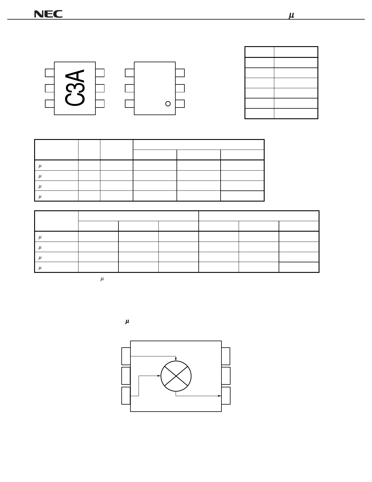
PIN FUNCTIONS (Pin Voltage is measured at VCC = VPS = VRFOUT = 2.8V)
Pin Pin Applied Pin
Function and Explanation
No. Name Voltage Voltage
(V)
(V)
1 IFinput
—
1.2
This pin is the IF input pin to the double balanced
mixer (DBM). The input is designed as a high
impedance. The circuit helps suppress spurious
signals. Also this symmetrical circuit can keep
specified performance insensitive to process-
condition distribution. For that reason, a double
balanced mixer is adopted.
3
2 GND
GND
—
GND pin. Ground pattern on the board should be
4
formed as wide as possible. Track length should
be kept as short as possible to minimize ground
inductance.
3 LOinput
–
2.1
5
VCC 2.7 to 3.3 —
6 RFoutput Same bias —
as VCC
through
external
inductor
Local input pin. Recommended input level is -10
to 0 dBm.
Supply voltage pin.
This pin is the RF output from the double
balanced mixer. This pin is designed as an open
collector. Due to the high impedance output, this
pin should be externally equipped with an LC
matching circuit to the next stage.
Equivalent Circuit
5
6
1
2
Share Link: