69190-405 Ver la hoja de datos (PDF) - Impala Linear Corporation
Número de pieza
componentes Descripción
Fabricante
69190-405 Datasheet PDF : 16 Pages
| |||
150mA SOT-23 Ultra Low Noise CMOS RF-LDO™ Regulator
Input Capacitor
An input capacitor CIN of value 1µF or larger should be con-
nected from VIN to the main ground plane. This will help to
filter supply noise from entering the LDO. The input capaci-
tor should be connected as close to the LDO regulator input
pin as is practical. Using a high-value input capacitor will
offer superior line transient response as well as better pow-
er supply ripple rejection. A ceramic or tantalum capacitor
may be used at the input of the LDO regulator.
Note that there is a parasitic diode from the LDO regulator
output to the input. If the input voltage swings below the reg-
ulator’s output voltage by a couple of hundred milivolts then
the regulator may be damaged. This condition must be
avoided. In many applications a large value input capacitor,
CIN, will hold VIN higher than VOUT and decay slower than VOUT
when the LDO is powered off.
Output Capacitor Selection
Impala strongly recommends the use of low ESR (equiva-
lent series resistance) ceramic capacitors for COUT and
CNOISE The ILC7082 is stable with low ESR capacitor (as low
as zero Ω). The value of the output capacitor should be 1µF
or higher. Either ceramic chip or a tantalum capacitor may
be used at the output.
Use of ceramic chip capacitors offer significant advantages
over tantalum capacitors. A ceramic capacitor is typically
cheaper than a tantalum capacitor, it usually has a smaller
footprint, lower height, and lighter weight than a tantalum
capacitor. Furthermore, unlike tantalum capacitors which are
polarized and can be damaged if connected incorrectly,
ceramic capacitors are non-polarized. Low value ceramic
chip capacitors with X5R or X7R dielectric are available in
the 100pF to 4.7mF range. Beware of using ceramic capaci-
tors with Y5V dielectric since their ESR increases significant-
ly at cold temperatures. Figure 12 shows a list of recom-
mended ceramic capacitors for use at the output of ILC7082.
Note: If a tantalum output capacitor is used then for stable
operation Impala recommends a low ESR tantalum capaci-
tor with maximum rated ESR at or below 0.4W. Low ESR
tantalum capacitors, such as the TPS series from AVX
Corporation (www.avxcorp.com) or the T495 series from
Kemet (www.kemet.com) may be used.
In applications where a high output surge current can be expect-
ed, use a high value but low ESR output capacitor for superior
load transient response. The ILC7082 is stable with no load.
Noise Bypass Capacitor
In low noise applications, the self noise of the ILC7082 can
be decreased further by connecting a capacitor from the
noise bypass pin (pin 4) to ground (pin 2). The noise bypass
pin is a high impedance node as such care should be taken
in printed circuit board layout to avoid noise pick-up from
external sources. Moreover, the noise bypass capacitor
should have low leakage.
Noise bypass capacitors with a value as low as 470pF may
be used. However, for optimum performance, use a 0.01mF
or larger, ceramic chip capacitor. Note that the turn on and
turn off response of the ILC7082 is inversely proportional to
the value of the noise bypass capacitor. For fast turn on and
turn off, use a small value noise bypass capacitor. In appli-
cations were exceptionally low output noise is not required,
consider omitting the noise bypass capacitor altogether.
The Effects of ESR (Equivalent Series Resistance)
The ESR of a capacitor is a measure of the resistance due
to the leads and the internal connections of the component.
Typically measured in mΩ (milli-ohms) it can increase to
ohms in some cases.
Wherever there is a combination of resistance and current,
voltages will be present. The control functions of LDOs use
two voltages in order to maintain the output precisely; VOUT
and VREF.
With reference to the block diagram in figure 4, VOUT is fed
back to the error amplifier and is used as the supply voltage
for the internal components of the ILC7082. So any change
in VOUT will cause the error amplifier to try to compensate to
maintain VOUT at the set level and noise on VOUT will be
reflected into the supply of each internal components of the
ILC7082. So any change in VOUT will cause the error ampli-
fier to try to compensate to maintain VOUT at the set level and
noise on VOUT will be reflected into the supply of each inter-
nal circuit. The reference voltage, VREF, is influenced by the
CNOISE pin. Noise into this pin will add to the reference volt-
age and be fed through the circuit. These factors will not
cause a problem if some simple steps are taken. Figure 5
shows where these added ESR resistances are present in
the typical LDO circuit.
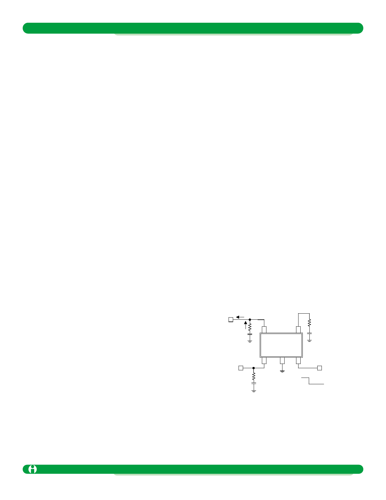
VOUT IOUT
IC
COUT
RC 5 SOT-23-5
4
ILC7082
R*
CNOISE
VIN
1
23
R*
CIN
RF LDOTM
Regulator
ON
OFF
Figure 5: ESR present in COUT and CNOISE
With this in mind low ESR components will offer better per-
formance where the LDO may be subjected to large load
transients current. ESR is less of a problem with CIN as the
voltage fluctuations at the input will be filtered by the LDO.
Impala Linear Corporation
ILC7082 1.3
(408) 574-3939 www.impalalinear.com
April 1999 7
Share Link: 