69190-405 Ver la hoja de datos (PDF) - Impala Linear Corporation
Número de pieza
componentes Descripción
Fabricante
69190-405 Datasheet PDF : 16 Pages
| |||
150mA SOT-23 Ultra Low Noise CMOS RF-LDO™ Regulator
ELECTRICAL CHARACTERISTICS ILC7082AIM5 (continued)
Shutdown (ON/OFF) Operation
The ILC7082 output can be turned off by applying 0.4V or
less to the device’s ON/OFF pin (pin 3). In shutdown mode,
the ILC7082 draws less than 1mA quiescent current. The
output of the ILC7081 is enabled by applying 1.5V to 13V at
the ON/OFF pin. In applications were the ILC7082 output
will always remain enabled, the ON/OFF pin may be con-
nected to VIN (pin 1). The ILC7082’s shutdown circuitry
includes hysteresis, as such the device will operate proper-
ly even if a slow moving signal is applied to the ON/OFF pin.
The device’s shutdown pin includes a 2MW internal pull
down resistor connected to ground.
Short Circuit Protection
The ILC7082 output can withstand momentary short circuit
to ground. Moreover, the regulator can deliver very high out-
put peak current due to its 1A instantaneous short circuit
current capability.
Thermal Protection
The ILC7082 also includes a thermal protection circuit
which shuts down the regulator when die temperature
exceeds 170°C due to overheating. In thermal shutdown,
once the die temperature cools to below 160°C, the regula-
tor is enabled. If the die temperature is excessive due to
high package power dissipation, the regulator’s thermal cir-
cuit will continue to pulse the regulator on and off. This is
called thermal cycling.
Excessively high die temperature may occur due to high dif-
ferential voltage across the regulator or high load current or
high ambient temperature or a combination of all three.
Thermal protection protects the regulator from such fault
conditions and is a necessary requirement in today’s
designs. In normal operation, the die temperature should be
limited to under 150°C.
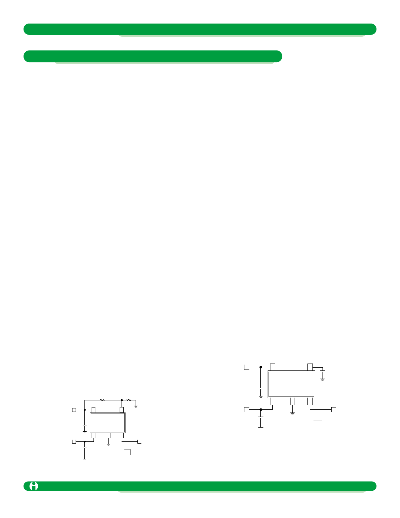
Adjustable Output Voltage
Figure 5 shows how an adjustable output voltage can be
easily achieved using ILC7082-Adj. The output voltage,
VOUT is given by the following equation:
VOUT = 1.24V x (R1/R2 + 1)
VOUT
R1
R2
5 SOT23-5 4 VADJ
COUT
VIN
CIN
ILC7082-ADJ
1
23
ON
OFF
For best results, a resistor value of 470kW or less may be
used for R2. The output voltage can be programmed from
2.5V to 12V.
Note that an external capacitor should not be connect-
ed to the adjustable feedback pin (pin 4). Connecting
an external capacitor to pin 4 may cause regulator
instability and lead to oscillations.
Maximum Output Current
The maximum output current available from the ILC7082 is
limited by the maximum package power dissipation as well
as the device’s internal current limit. For a given ambient
temperature, TA, the maximum package power dissipation
is given by:
PD(MAX) = (TJ(MAX) - TA) / θJA
where TJ(MAX) = 150°C is the maximum junction temperature
and θJA = 333°C/W is the package thermal resistance. For
example at TA = 85°C ambient temperature, the maximum
package power dissipation is;
PD(MAX) = 195mW.
The maximum output current can be calculated from the fol-
lowing equation:
IOUT(MAX) < PD(MAX) / (VIN - VOUT)
For example at VIN = 6V, VOUT = 5V and TA = 85°C, the max-
imum output current is IOUT(MAX) < 195mA. At higher output
current, the die temperature will rise and cause the thermal
protection circuit to be enabled.
APPLICATION HINTS
Figure 4 shows the typical application circuit for the ILC7082.
VOUT
COUT
5 SOT23-5 4
ILC7082
CNOISE
VIN
1
CIN
23
ON
OFF
Figure 4: Basic application circuit for fixed
output voltage versions
Fig. 3: Application circuit for adjustable output voltage
Impala Linear Corporation
ILC7082 1.3
(408) 574-3939
www.impalalinear.com
April 1999 6
Share Link: 