QL6325-E Ver la hoja de datos (PDF) - QuickLogic Corporation
Número de pieza
componentes Descripción
Fabricante
QL6325-E Datasheet PDF : 56 Pages
| |||
QL6325E Eclipse-E Data Sheet Rev. F
become a greater issue with specific requirements for setup, hold, clock to out, and switching times. Eclipse-
E has addressed these new system requirements and now includes a completely new I/O cell which consists
of programmable I/Os as well as a new cell structure consisting of three registers—Input, Output, and OE.
Eclipse-E offers banks of programmable I/Os that address many of the bus standards that are popular today.
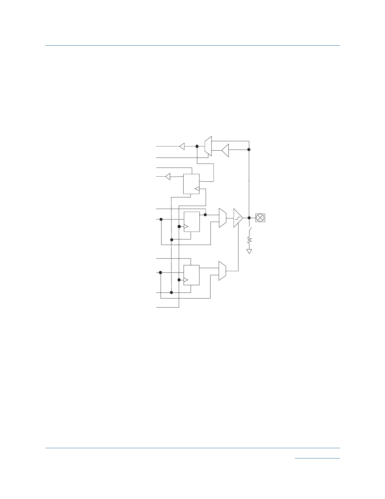
As shown in Figure 7 each bi-directional I/O pin is associated with an I/O cell which features an input register,
an input buffer, an output register, a three-state output buffer, an output enable register, and 2 two-to-one
output multiplexers.
Figure 7: Eclipse-E I/O Cell
+
-
INPUT
REGISTER
QE
D
R
PAD
OUTPUT
Q
D
REGISTER
R
OUTPUT ENABLE
REGISTER
EQ
D
R
The bi-directional I/O pin options can be programmed for input, output, or bi-directional operation. As shown
in Figure 7, each bi-directional I/O pin is associated with an I/O cell which features an input register, an input
buffer, an output register, a three-state output buffer, an output enable register, and 2 two-to-one multiplexers.
The select lines of the two-to-one multiplexers are static and must be connected to either VCC or GND.
For input functions, I/O pins can provide combinatorial, registered data, or both options simultaneously to the
logic array. For combinatorial input operation, data is routed from I/O pins through the input buffer to the
array logic. For registered input operation, I/O pins drive the D input of input cell registers, allowing data to
be captured with fast set-up times without consuming internal logic cell resources. The comparator and
multiplexor in the input path allows for native support of I/O standards with reference points offset from
traditional ground.
For output functions, I/O pins can receive combinatorial or registered data from the logic array. For
combinatorial output operation, data is routed from the logic array through a multiplexer to the I/O pin. For
registered output operation, the array logic drives the D input of the output cell register which in turn drives
© 2005 QuickLogic Corporation
www.quicklogic.com
•
•••
••
9
Share Link: 