QL6325-E Ver la hoja de datos (PDF) - QuickLogic Corporation
Número de pieza
componentes Descripción
Fabricante
QL6325-E Datasheet PDF : 56 Pages
| |||
QL6325E Eclipse-E Data Sheet Rev. F
PLL Signals
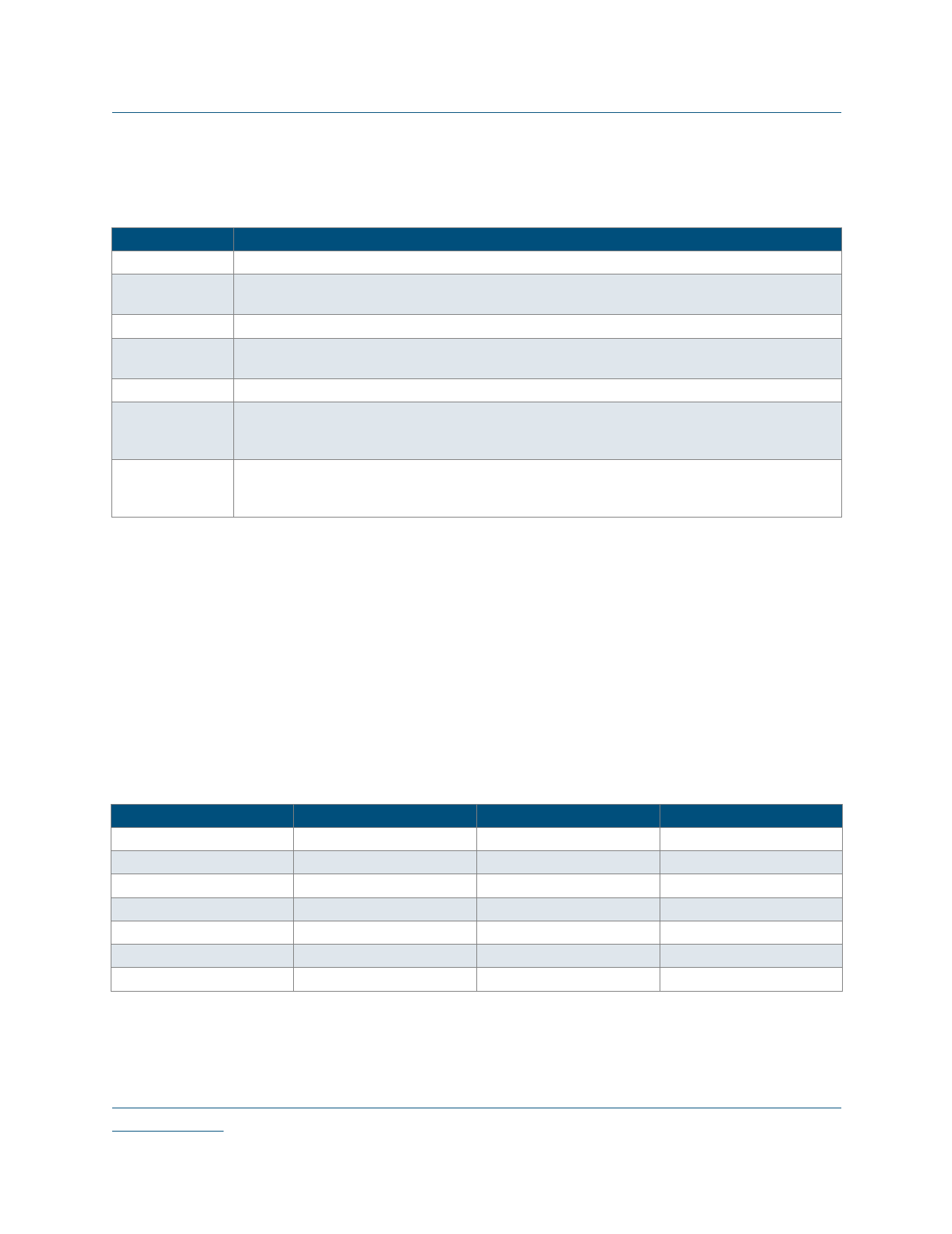
Table 5 summarizes the key signals in QuickLogic PLLs.
Table 5: QuickLogic PLL Signals
Signal Name
Description
PLLCLK_IN Input clock signal.
PLL_RESET
Active High Reset If PLL_RESET is asserted, then CLKNET_OUT and PLLPAD_OUT are reset
to 0. This signal must be asserted and then released in order for the LOCK_DETECT to work.
ONn_OFFCHIP This is a reserved signal. It can be connected to VCC or GND.
CLKNET_OUT
Out to internal gates This signal bypasses the PLL logic before driving the clock tree. Note that
this signal cannot be used in the same quadrant where the PLL signal is used (PLLCLK_OUT).
PLLCLK_OUT Out from PLL to internal gates This signal can drive the clock tree after going through the PLL.
PLLPAD_OUT
Out to off-chip This outgoing signal is used off-chip. The PLLPAD_OUT is always active, driving
the PLL-derived clock signal out through the pad. The PLLPAD_OUT will not oscillate if
PLL_RESET is asserted, or if the PLL is powered down.
Active High Lock detection signal
LOCK_DETECT NOTE: For simulation purposes, this signal gets asserted after 10 clock cycles. However, it can take
a maximum of 200 clock cycles to sync with the input clock upon release of the PLL_RESET signal.
NOTE: Because PLLCLK_IN and PLL_RESET signals have PLL_INPAD, and PLLPAD_OUT has OUTPAD,
you do not need to add additional pads to your design.
I/O Cell Structure
Eclipse-E features a variety of distinct I/O pins to maximize performance, functionality, and flexibility with
bi-directional I/O pins and input-only pins. All input and I/O pins are 1.8 V, 2.5 V, and 3.3 V tolerant and
comply with the specific I/O standard selected. For single ended I/O standards, VCCIO specifies the input
tolerance and the output drive. For voltage referenced I/O standards (e.g SSTL), the voltage supplied to the
INREF pins in each bank specifies the input switch point. For example, the VCCIO pins must be tied to a 3.3 V
supply to provide 3.3 V compliance. Eclipse-E can also support the LVDS and LVPECL I/O standards with
the use of external resistors (see Table 6).
I/O Standard
LVTTL
LVCMOS25
LVCMOS18
PCI
GTL+
SSTL3
SSTL2
Table 6: I/O Standards and Applications
Reference Voltage
n/a
n/a
n/a
n/a
1
1.5
1.25
Output Voltage
3.3 V
2.5 V
1.8 V
3.3 V
n/a
3.3 V
2.5 V
Application
General Purpose
General Purpose
General Purpose
PCI Bus Applications
Backplane
SDRAM
SDRAM
As designs become more complex and requirements more stringent, several application-specific I/O standards
have emerged for specific applications. I/O standards for processors, memories, and a variety of bus
applications have become commonplace and a requirement for many systems. In addition, I/O timing has
8
•
•••
••
www.quicklogic.com
© 2005 QuickLogic Corporation
Share Link: 