QL6325-E Ver la hoja de datos (PDF) - QuickLogic Corporation
Número de pieza
componentes Descripción
Fabricante
QL6325-E Datasheet PDF : 56 Pages
| |||
QL6325E Eclipse-E Data Sheet Rev. F
Fin represents a very stable high-frequency input clock and produces an accurate signal reference. This signal
can either bypass the PLL entirely, thus entering the clock tree directly, or it can pass through the PLL itself.
Within the PLL, a voltage-controlled oscillator (VCO) is added to the circuit. The external Fin signal and the
local VCO form a control loop. The VCO is multiplied or divided down to the reference frequency, so that a
phase detector (the crossed circle in Figure 6) can compare the two signals. If the phases of the external and
local signals are not within the tolerance required, the phase detector sends a signal through the charge pump
and loop filter (Figure 6). The charge pump generates an error voltage to bring the VCO back into alignment,
and the loop filter removes any high frequency noise before the error voltage enters the VCO. This new VCO
signal enters the clock tree to drive the chip's circuitry.
Fout represents the clock signal emerging from the output pad (the output signal PLLPAD_OUT is explained
in Table 5). The PLL always drives the PLLPAD_OUT signal, regardless of whether the PLL is configured for
on-chip use. The PLLPAD_OUT will not oscillate if PLL_RESET is asserted, or if the PLL is powered down.
Most QuickLogic products contain four PLLs. The PLL presented in Figure 6 controls the clock tree in the
fourth quadrant of its FPGA. QuickLogic PLLs compensate for the additional delay created by the clock tree
itself, as previously noted, by subtracting the clock tree delay through the feedback path.
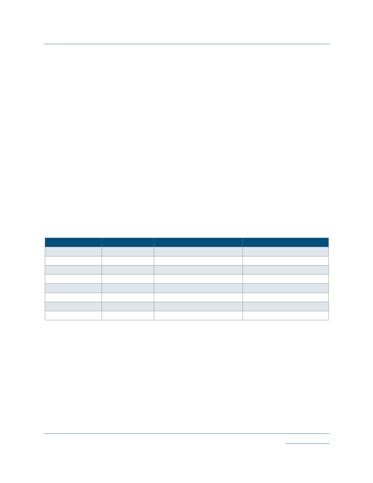
PLL Modes of Operation
QuickLogic PLLs have eight modes of operation, based on the input frequency and desired output frequency—
Table 4 indicates the features of each mode.
NOTE: “HF” stands for “high frequency” and “LF” stands for “low frequency.”
Table 4: PLL Mode Frequencies
PLL Model
PLL_HF
PLL_LF
PLL_MULT2HF
PLL_MULT2LF
PLL_DIV2HF
PLL_DIV2LF
PLL_MULT4
PLL_DIV4
Output Frequency
Same as input
Same as input
2x
2x
1/2x
1/2x
4x
1/4x
Input Frequency Range
66 MHz–220 MHz
25 MHz–66 MHz
33 MHz–110 MHz
12.5 MHz–33 MHz
220 MHz–440 MHz
50 MHz–220 MHz
12.5 MHz–50 MHz
100 MHz–440 MHz
Output Frequency Range
66 MHz–220 MHz
25 MHz–66 MHz
66 MHz–220 MHz
25 MHz–66 MHz
110 MHz–220 MHz
25 MHz–110 MHz
50 MHz–200 MHz
25 MHz–110 MHz
The input frequency can range from 12.5 MHz to 440 MHz, while output frequency ranges from 25 MHz to
220 MHz. When adding PLLs to the top-level design, be sure that the PLL mode matches the desired input
and output frequencies.
© 2005 QuickLogic Corporation
www.quicklogic.com
•
•••
••
7
Share Link: 