QL6325-E-7PQ208M Ver la hoja de datos (PDF) - QuickLogic Corporation
Número de pieza
componentes Descripción
Fabricante
QL6325-E-7PQ208M Datasheet PDF : 56 Pages
| |||
RESET
S1
S2
S3
CIN
SIGN1
SIGN2
A[7:0]
A[15:8]
A[0:15]
CLK
B[0:15]
QL6325E Eclipse-E Data Sheet Rev. F
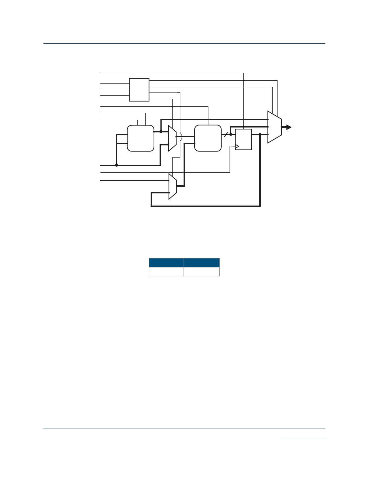
Figure 5: ECU Block Diagram
D
C
3-4
decoder
B
A
8-bit
2-1
Multiplier
mux
16-bit
Adder
DQ
17-bit
Register
00
01 3-1
mux
10
Q[16:0]
2-1
mux
The Eclipse-E ECU block (Table 2) is placed next to the SRAM circuitry for efficient memory/instruction fetch
and addressing for DSP algorithmic implementations.
Table 2: Eclipse-E ECU Block
Device
QL6325E
ECUs
12
Up to twelve 8-bit MAC functions can be implemented per cycle for a total of 1.2 billion MACs/s when clocked
at 100 MHz. Additional multiply-accumulate functions can be implemented in the programmable logic.
The modes for the ECU block are dynamically re-programmable through the programmable logic.
© 2005 QuickLogic Corporation
www.quicklogic.com
•
•••
••
5
Share Link: 