QL6325-E Ver la hoja de datos (PDF) - QuickLogic Corporation
Número de pieza
componentes Descripción
Fabricante
QL6325-E Datasheet PDF : 56 Pages
| |||
QL6325E Eclipse-E Data Sheet
• • • • • • FPGA Combining Performance, Density, and Embedded RAM
Device Highlights
Flexible Programmable Logic
• 0.18 µm six layer metal CMOS process
• 1.8/2.5/3.3 V drive capable I/O
• 1536 logic cells
• Up to 4,002 flip-flops
• Up to 310 I/O pins
• Up to 335 user-available pins
• 320,460 maximum system gates
Embedded Dual Port SRAM
• Twenty-four 2,304-bit dual port high
performance SRAM blocks
• 55,296 RAM bits
• RAM/ROM/FIFO wizard for automatic
configuration
• Configurable and cascadable
Programmable I/O
• High performance I/O cell
• Programmable slew rate control
• Programmable I/O standards:
LVTTL, LVCMOS, LVCMOS18, PCI, GTL+,
SSTL2, and SSTL3
Eight independent I/O banks
Three register configurations: Input, Output,
and Output Enable
Advanced Clock Network
• Nine global clock networks:
One dedicated
Eight programmable
• 20 quad-net networks—five per quadrant
• 16 I/O controls—two per I/O bank
• Four phase locked loops
Embedded Computational Units
Twelve ECUs provide integrated Multiply, Add, and
Accumulate functions.
Security Features
The QuickLogic products come with secure
ViaLink technology that protects intellectual
property from design theft and reverse engineering.
No external configuration memory needed;
instant-on at power-up.
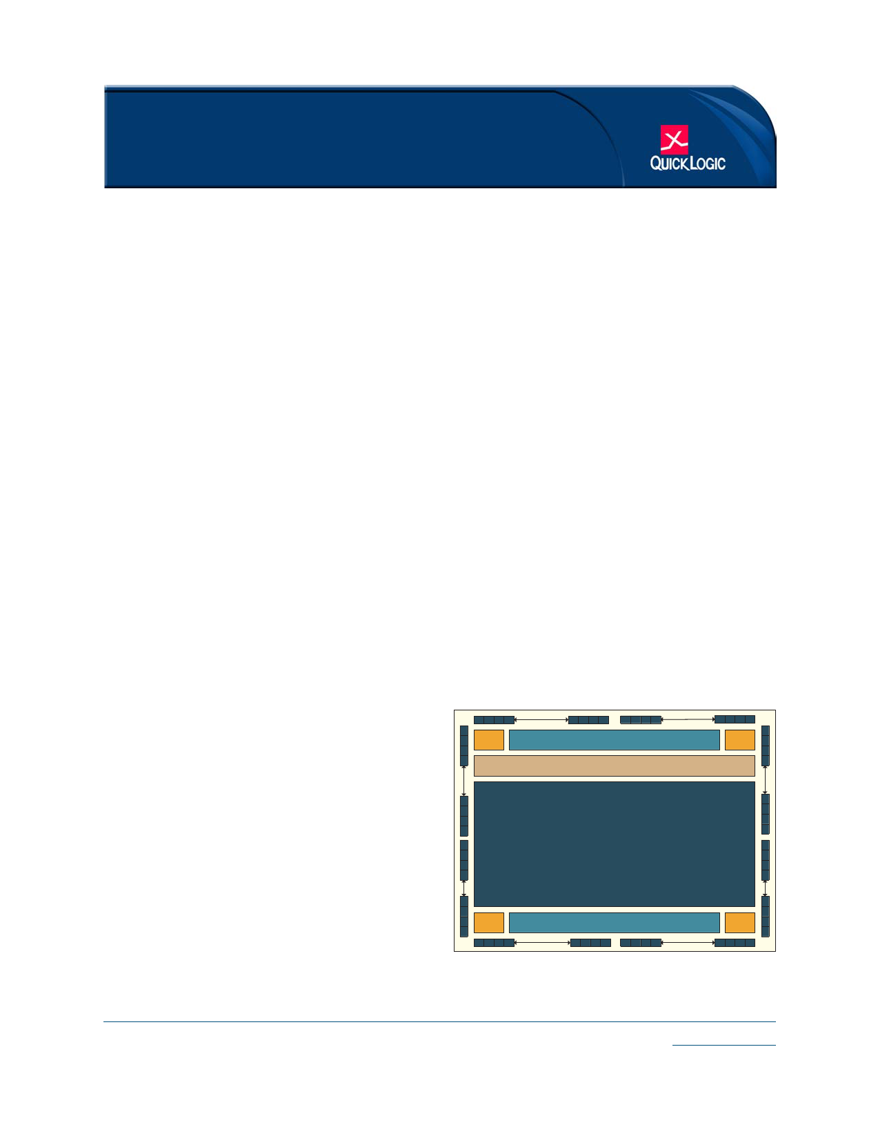
Figure 1: QL6325E Eclipse-E Block Diagram
PLL
Embedded RAM Blocks
PLL
Embeded Computational Units
Fabric
PLL
Embedded RAM Blocks
PLL
© 2005 QuickLogic Corporation
www.quicklogic.com
•
•••
••
1
Share Link: 