EL1056 Ver la hoja de datos (PDF) - Intersil
Número de pieza
componentes Descripción
Fabricante
EL1056 Datasheet PDF : 12 Pages
| |||
EL1056A, EL1056
Logic Inputs
The logic inputs are all differential types, with both NPN and
PNP transistors connected to each terminal. They are
optimized for differential ECL drive, which optimizes + to -
edge delay time matching. Larger logic levels can introduce
feedthrough glitches into the output waveform. For CMOS
input logic levels, an ECL output waveform will show
feedthrough when the input risetime is shorter than 8ns,
differential or single-ended. CMOS output swings show less
aberration, and the EL1056 can tolerate a 4ns single-ended
risetime or 2ns risetime for differential inputs. Attenuating
CMOS or TTL inputs to 1VPP will eliminate all logic
feedthrough as shown in Figure 1.
FIGURE 1. ALTERNATE LOGIC INTERFACE
Slewrate Control
The slewrate is controlled by the ISR input. This is a current
input and scales the output slewrate by a nominal
1.25V/ns/mA. The slewrate maintains calibration and
symmetry to at least as slow as 0.2V/ns. The practical upper
end of ISR is 1mA, and supply current increases with
increasing ISR.
The ISR control can be used to adjust individual pin drivers
to a system standard, by adjusting the value of its series
resistor. Slewrate can also be slowed to reduce output
ringing and crosstalk.
With ECL output swings, there is not enough voltage
excursion to incur slewrate delays to 50% logic threshold.
The risetime, delays, and dispersions do not degrade with
reasonably reduced ISR, and overshoot will reduce
markedly. An ISR of 350µA produces a very good ECL
output, and driver dissipation is also reduced.
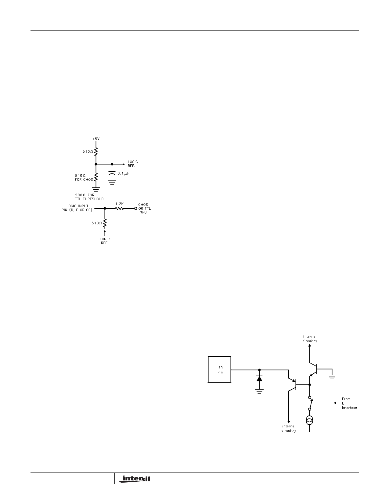
The ISR pin is connected to the emitter of a PNP transistor
whose base is biased a diode below ground (see Figure 2).
Thus, the ISR input looks like a low impedance for positive
input currents, and is biased close to ground. A protection
diode absorbs negative currents, and the input PNP will not
conduct. In power-down mode, the PNP releases its current
sink and the external circuit must not present more than 6V
to the disabled ISR input, or emitter-base damage to the
NPN will occur within the driver. A signal diode or zener can
be used to clamp the ISR input for positive input voltages if
the voltage on the ISR resistor is potentially greater than 6V
when the driver is in power-down mode.
Output Stage–Three-State Mode
In three-state mode (OE low) the output transistors have
their emitter-base junctions reverse-biased by a diode
voltage. This turn-off voltage is in fact provided by an internal
buffer whose input is connected to the output pin (see Figure
3). Transistors Q1–Q4 form the output buffer in normal
mode. The three-state mode buffer Q5–Q8 replicates
externally impressed voltages from the output pin onto the
internal schottky switch node. They also turn off Q1–Q4 by a
reverse diode voltage between bases and emitters,
effectively bootstrapping the internal voltages, so that no
transistor's base-emitter junction is reverse-biased by a
damaging potential. Another benefit is that the capacitance
seen at the output in three-state mode is reduced.
Because the three-state buffer's input is connected to the
output terminal, the output is quite “alive” during three-state.
For instance, the input bias current of the buffer is seen as
the three-state “leakage”, and its variation with applied
voltage becomes three-state input impedance.
The three-state input current is like a current source, and it
can drag an output to unpredictable voltages. It is not a
danger to connect a three-stated output that has drifted to,
say, -6V to a logic pin of a device to be tested. The three-
state output current will simply comply with whatever voltage
the connected part normally establishes.
The three-state input impedance is also quite active over
frequency. The output can oscillate when presented with
resonant or inductive impedances. To prevent this, a snubber
should be connected from output to ground, consisting of a
resistor in series with a small capacitor. The snubber can
also reduce the reflections of the coaxial line when driven
from the far end, since the line appears to have an open
termination during three-state. Typical values for the resistor
are 50Ω to 75Ω, and 12pF to 22pF for the series capacitor.
The effect of the snubber is to “de-Q” resonances at the
output.
FIGURE 2. ISR PIN CIRCUITRY
9
Share Link: 