EB201 Ver la hoja de datos (PDF) - ON Semiconductor
Número de pieza
componentes Descripción
Fabricante
EB201 Datasheet PDF : 8 Pages
| |||
STANDARD
TMOS
CELL
DENSITY
EB201/D
HDTMOS
CELL
DENSITY
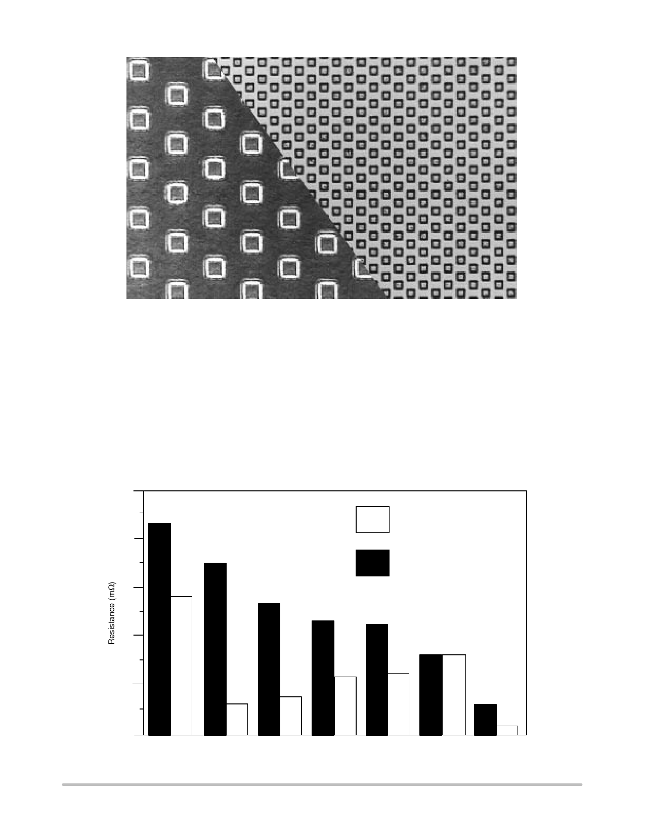
Figure 2. HDTMOS versus Standard TMOSE Cell Densities
Also a key factor in lowering on–resistance is the use of
low resistivity substrates. The substrate of the power
MOSFET can be thought of as the mechanical base onto
which the transistors are built. Although it comprises almost
all of the wafer thickness, its only purpose is to strengthen
the wafer for its trip through wafer processing, dicing, and
final assembly. The resistance added by the substrate is
entirely undesirable, and low resistivity substrates are a must
for ultra–low on–resistance MOSFETs. Figure 3 compares
the major on–resistance components of HDTMOS to those
of standard cell MOSFETs.
The on–resistance area product is a good figure of merit
for the power MOSFET, and lower is better for this
parameter. The original 28 mΩ, 60 V MOSFET had an
on–resistance area product of about 7.0 mΩ–cm2 (based on
the maximum on–resistance rating at 25°C). Die size
reductions over the last several years have shaved the
product to about 5.5 mΩ–cm2. The newest device, the
MTP75N05HD, is more than a refinement of typical power
MOSFET technology. Its 2.4 mΩ–cm2 product was
attained by completely redesigning the device and
developing an entirely new manufacturing process.
5
ÉÉÉÉÉÉHDTMOS
4
STD TMOS
3
2
1
0
ÈÈÈÈÈÈÈÈÈÈÈÈÈÈÈÈÈÈÈÈ ÈÈÈÈÈÈÈÈÈ ÈÈÈÈÈÈ ÈÈÈÈÈÈÈÈÈÈ ÈÈÈÈÈÈÈÈÈÈÈÈÈÈÈ ÈÈÈÈÈÈÈÈÈÈÈÈ ÉÉÉÉ
SPREAD
SUB
JFET
WIRE
CHAN
METAL
ACCUM
Figure 3. On–Resistance Components
http://onsemi.com
2
Share Link: 