DRF100 Ver la hoja de datos (PDF) - Advanced Power Technology
Número de pieza
componentes Descripción
Fabricante
DRF100 Datasheet PDF : 12 Pages
| |||
DRF100
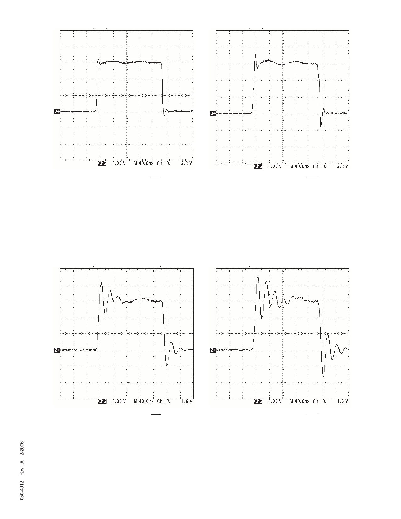
Figure 13, Anti-Ring ON
Figure 14, Anit-RIng OFF
The output waveform with the Anti-Ring function ON is illustrated in Figure 13 and the
Anti-Ring function OFF is illustrated in Figure 14. The load is 50Ω with no load capacitance,
other than the output capacitance of the driver.
Figure 15, Anti-Ring ON
Figure 16, Anit-RIng OFF
The output waveform with the Anti-Ring function ON is illustrated in Figure 15 and the
Anti-Ring function OFF is illustrated in Figure 16. The load is 50Ω + 3nF of capacitance.
The ring amplitude in Figure 15 is clearly above the 2-4V threshold voltage of most power
MOSFETs, while In Figure 16 we see that the ring peak is at ~=2V, also see Figure 13. It
is most likely that the wave form of Figure 16 will cause a cross conduction in a Bridge or
push pull topology.
Share Link: 