HDMP-1546 Ver la hoja de datos (PDF) - HP => Agilent Technologies
Número de pieza
componentes Descripción
Fabricante
HDMP-1546 Datasheet PDF : 15 Pages
| |||
Output Jitter Characteristics
TA = 25°C, VCC = 3.3 V
Symbol
Parameter
RJ[1]
Random Jitter at DOUT, the High Speed Electrical Data Port, specified as
1 sigma deviation of the 50% crossing point (RMS)
DJ[1] Deterministic Jitter at DOUT, the High Speed Electrical Data Port (pk-pk)
Units
ps
ps
Typ.
8
15
Note:
1. Defined by Fibre Channel Specification Rev 4.1, Annex A, Section A.4 and tested using measurement method shown in Figure 8.
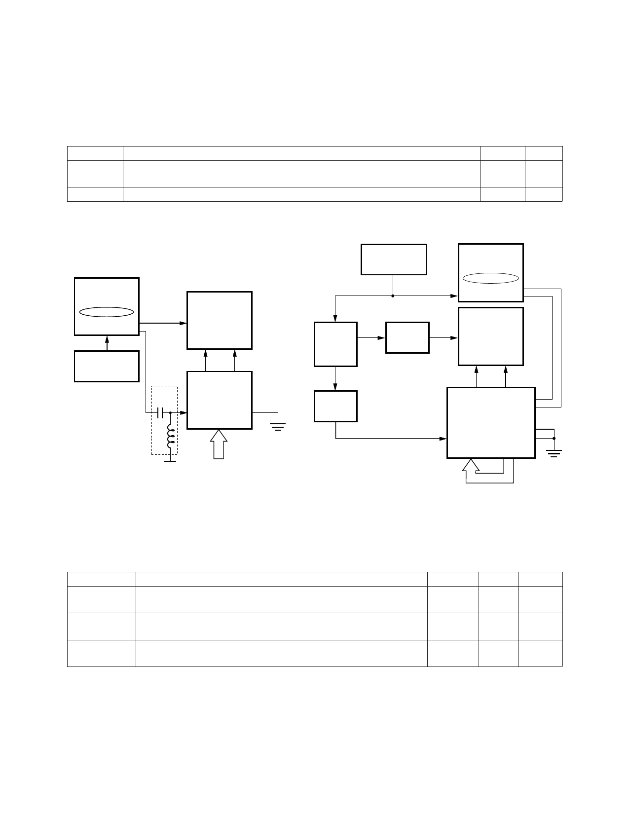
HP70841B
PATTERN
GENERATOR*
0000011111
+ DATA
- DATA
106.25 MHz
1.0625 GHz
HP83480A
OSCILLOSCOPE
TRIGGER
CH1 CH2
HP70311A
CLOCK SOURCE
* PATTERN
GENERATOR
PROVIDES A
DIVIDE BY
10 FUNCTION.
BIAS
TEE
+DOUT -DOUT
HDMP-1536
REFCLK LOOPEN
Tx[0..9]
1.4 V
0011111000
(STATIC K28.7)
HP70311A
CLOCK SOURCE
DIVIDE
BY 10
CIRCUIT
(DUAL
OUTPUT)
1.25 GHz
DIVIDE
BY 2
CIRCUIT
HP70841B
PATTERN
GENERATOR
+K28.5, -K28.5
+ DATA
- DATA
HP83480A
OSCILLOSCOPE
TRIGGER
CH1 CH2
VARIABLE
DELAY
TTL
125 MHz
+DOUT -DOUT
-DIN
+DIN
HDMP-1636
REFCLK
ENBYTSYNC
LOOPEN
Tx[0..9] Rx[0..9]
a. Block Diagram of RJ Measurement Method.
Figure 8. Transmitter Jitter Measurement Method.
b. Block Diagram of DJ Measurement Method.
Thermal and Power Temperature Characteristics,
TA[1] = 0°C to +60°C, VCC = 3.15 V to 3.45 V
Symbol
Parameter
PD,TRx[2,3]
Transceiver Power Dissipation, Outputs Open, Parallel Data
has 5 Ones and 5 Zeroes
PD,TRx[2,3,4] Transceiver Power Dissipation, Outputs Connected per
Recommended Bias Terminations with Idle Pattern
Θjc[5]
Thermal Resistance, Junction to Case HDMP-1536
HDMP-1546
Units
mW
mW
°C/Watt
Typ.
630
685
10
7
Max.
850
900
Notes:
1. Device tested and characterized under TA conditions specified, with TC monitored at approximately 20° higher than TA.
2. PD is multiplying the max VCC by the max ICC and subtracting the power dissipated outside the chip at the high speed bias resistors.
3. Typical specified with VCC = 3.3 volts, maximum specified with VCC = 3.45 volts.
4. Specified with high speed outputs biased with 150 Ω resistors and receiver TTL outputs driving 10 pF loads.
5. Based on independant package testing by HP. Θja for these devices is 48°C/Watt for the HDMP-1536 and 44°C/Watt for the
HDMP-1546. Θja is measured on a standard 3x3" FR4 PCB in a still air environment. To determine the actual junction temperature
in a given application, use the value as described as follows: Tj = TC + (Θjc x Pd), where TC is the case temperature measured on
the top center of the package and PD is the power being dissipated.
704
Share Link: 