CS51221 Ver la hoja de datos (PDF) - ON Semiconductor
Número de pieza
componentes Descripción
Fabricante
CS51221 Datasheet PDF : 14 Pages
| |||
CS51221
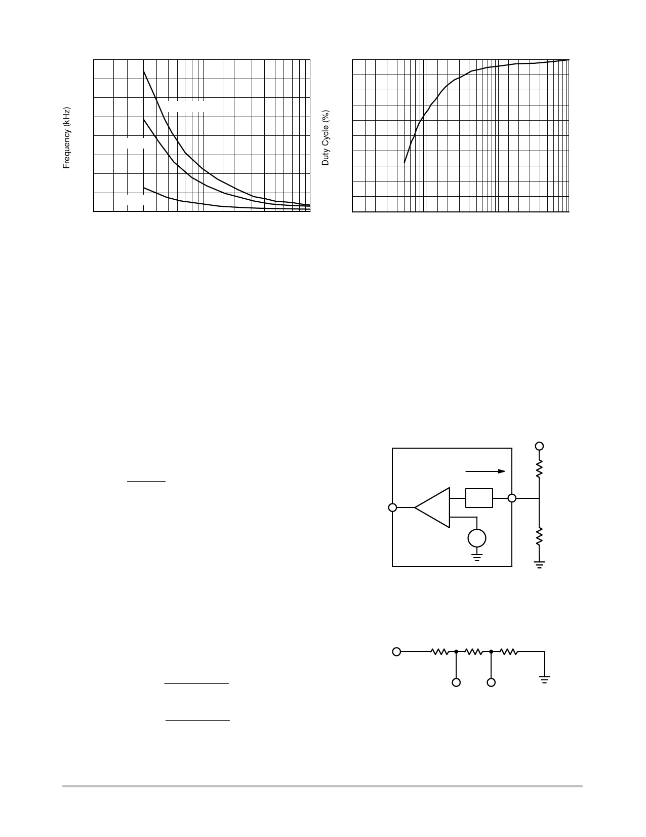
800
700
600
RT = 5.0 K
500
400
RT = 10 K
300
200
100
RT = 50 K
0
0.0001
0.001
0.01
CT (mF)
Figure 10. Typical Performance Characteristics,
Oscillator Frequency vs. CT
1.00
0.95
0.90
0.85
0.80
0.75
0.70
0.65
0.60
0.55
0.50
1000
10000
100000
RT (W)
1000000
Figure 11. Typical Performance Characteristics,
Oscillator Duty Cycle vs. RT
that during steady state, VCOMP doesn’t change for input
voltage variations. This intuitively explains why FF voltage
mode control has superior line regulation and line transient
response. Knowing the nominal value of VIN and TON, one
can also select the value of RC to place VCOMP at the center
of its dynamic range.
Select Feedback Voltage Divider
As shown in Figure 12, the voltage divider output feeds to
the FB pin, which connects to the inverting input of the error
amplifier. The non−inverting input of the error amplifier is
connected to a 1.27 V (typ) reference voltage. The FB pin
has an input current which has to be considered for accurate
DC outputs. The following equation can be used to calculate
the R1 and R2 value
ǒ Ǔ R2
R1 ) R2
VOUT
+ 1.27 * ʼn
where ∇ is the correction factor due to the existence of the
FB pin input current Ier.
ʼn + (Ri ) R1ńńR2)Ier
Ri = DC resistance between the FB pin and the voltage
divider output.
Ier = VFB input current, 1.3 mA typical.
Design Voltage Dividers for OV and UV Detection
In Figure 13, the voltage divider uses three resistors in
series to set OV and UV threshold seen from the input
voltage. The values of the resistors can be calculated from
the following three equations, where the third equation is
derived from OV hysteresis requirement.
ǒ Ǔ VIN(LOW)
R2 ) R3
R2 ) R3 ) R1
+ 1.0 V
(A)
ǒ Ǔ VIN(HIGH)
R3
R2 ) R3 ) R1
+ 2.0 V
(B)
12.5 mA (R1 ) R2) + VHYST
(C)
where:
VIN(LOW), VIN(HIGH) = input voltage OV and UV
threshold;
VHYST = OV hysteresis seen at VIN
It is self−evident from equation A and B that to use this
design, VIN(HIGH) has to be two times greater than
VIN(LOW). Otherwise, two voltage dividers have to be used
to program OV and UV separately.
COMP
VOUT
Ier
R1
FB
−
Ri
+
+
−
1.27
R2
Figure 12. The Design of Feedback Voltage Divider
Has to Consider the Error Amplifier Input Current
R1
R2
R3
VIN
VUV
VOV
Figure 13. OV/UV Monitor Divider
http://onsemi.com
11
Share Link: 