CMX602AP3 Ver la hoja de datos (PDF) - CML Microsystems Plc
Número de pieza
componentes Descripción
Fabricante
CMX602AP3 Datasheet PDF : 25 Pages
| |||
Calling Line Identifier
CMX602A
1.5 General Description
1.5.1 Mode Control Logic
The CMX602A's operating mode and the source of the DET and IRQN outputs are determined by the logic
levels applied to the MODE and ZP input pins;
ZP MODE
Mode
0
0 Tone Alert Detect
0
1 FSK Receive
DET o/p from
Tone Alert Signal
Detection
FSK Level Detector
1
0 'Zero-Power'
Ring or Line Polarity
Reversal Detector.
IRQN o/p from
Valid ‘off-hook’ CAS.
Ring or Line Polarity
Reversal Detector.
FSK Data Retiming [1].
Ring or Line Polarity
Reversal Detector.
Ring or Line Polarity
Reversal Detector.
1
1 'Zero-Power'
Ring or Line Polarity
-
Reversal Detector.
[1] If enabled.
In the 'Zero-Power' modes, power is removed from all of the internal circuitry except for the Ring or Line
Polarity Reversal Detector and the DET and IRQN outputs.
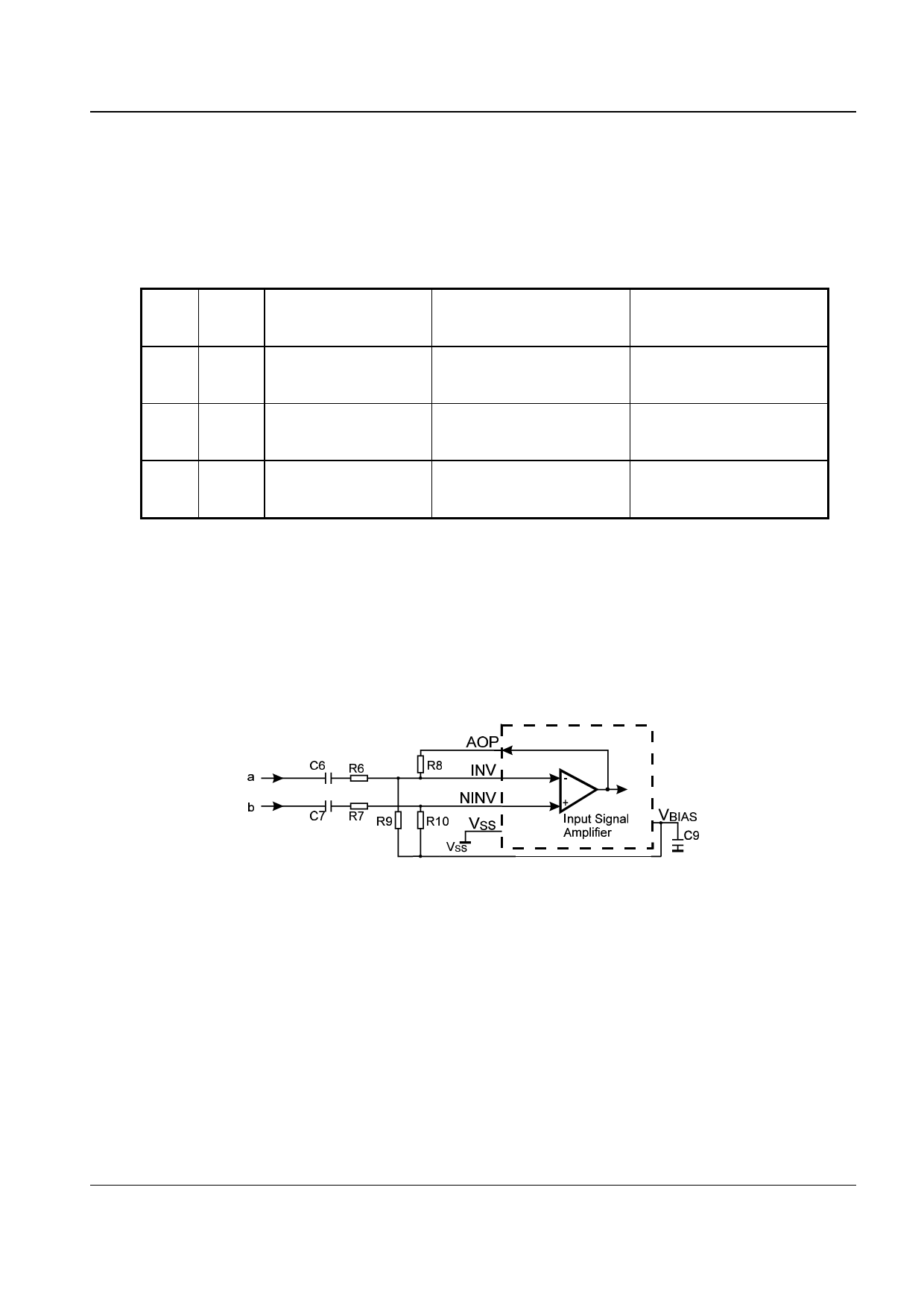
1.5.2 Input Signal Amplifier
This amplifier is used to convert the balanced FSK and Tone Alert signals received over the telephone line to
an unbalanced signal of the correct amplitude for the FSK receiver and Tone Alert Detector circuits.
Figure 3a : Input Signal Amplifier, balanced input configuration
The design equations for this circuit are;
Differential voltage gain VAOP / V(b-a) = R8/R6
R6 = R7 = 470kΩ
R10 = 160kΩ
R9 = R8 x R10 / (R8 - R10)
The target differential voltage gain depends on the expected signal levels between the A and B wires and the
CMX602A's internal threshold levels, which are proportional to the supply voltage.
© 1998 Consumer Microcircuits Limited
7
D/602A/4
Share Link: 