CGY0918 Ver la hoja de datos (PDF) - Siemens AG
Número de pieza
componentes Descripción
Fabricante
CGY0918 Datasheet PDF : 4 Pages
| |||
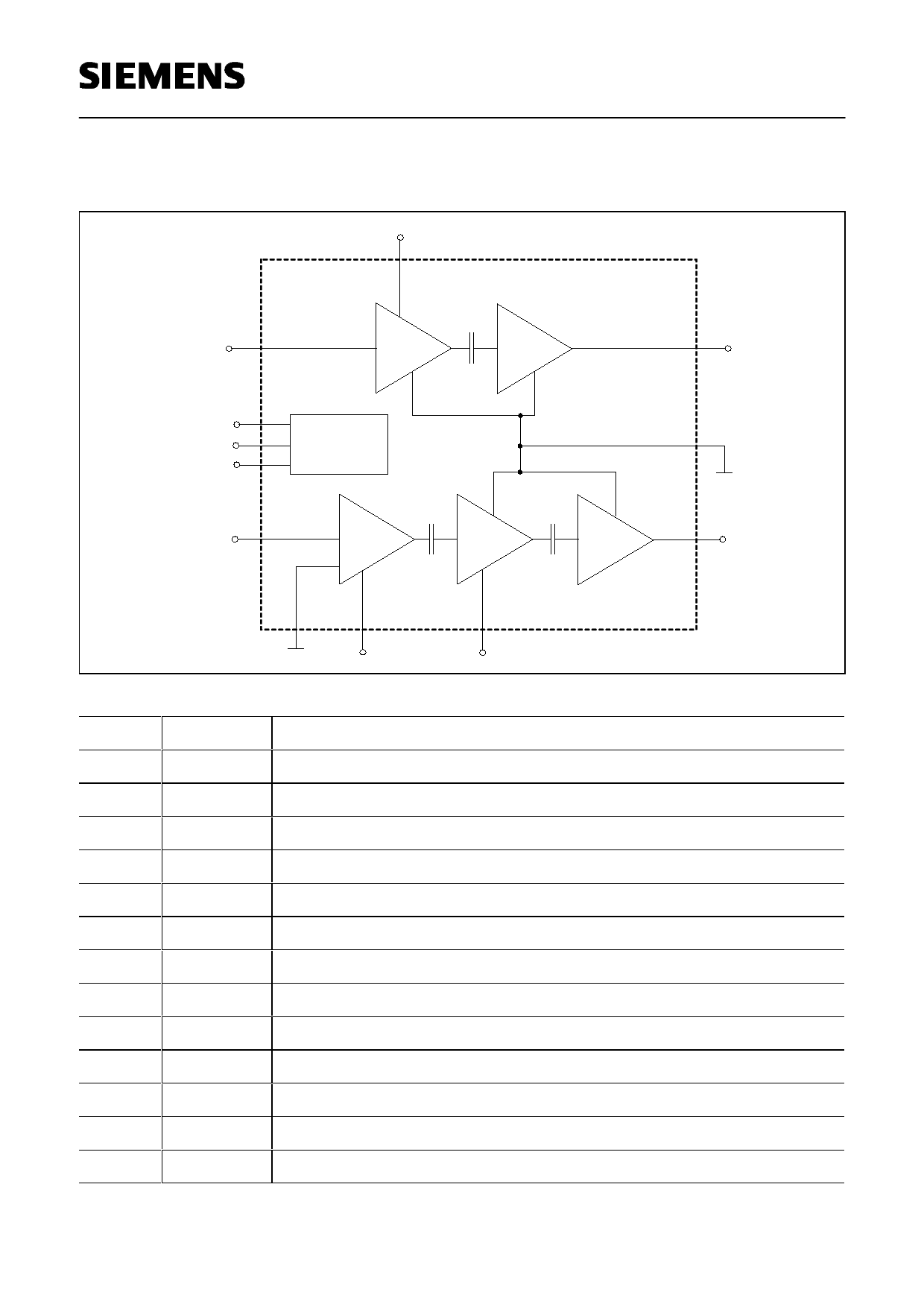
Functional block diagramm:
G_VD1
G_IN
G_Control
P_Control
Vneg
P_IN
current
control circuit
CGY 0918
CGY0918
G_OUT
GND
P_OUT
P_GND1
P VD1
P VD2
Pin #
Name Configuration
1
2
3
4
5,6,7,8
P_IN
P_GND1
P_VD1
P_VD2
P_OUT
RF input PCN
Ground 1st stage PCN
Drain 1st stage PCN
Drain 2nd stage
RF output PCN and drain 3rd stage
9
G_IN RF input GSM
10 G_Control Power control GSM
11 P_Control Power control PCN
12
Vneg Negative voltage for current control circuit
13
14
15,16
n.c.
G_VD1
G_OUT
-
Drain 1st stage GSM
RF output GSM and drain 2nd stage
(17)
GND2 Ground (backside of MW16 package)
Siemens Aktiengesellschaft
2
Semiconductor Group
2
23.07.98
HL HF19P9E8-G11a-A0s1
Share Link: 