CAV24C02WE-GT3 Ver la hoja de datos (PDF) - ON Semiconductor
Número de pieza
componentes Descripción
Fabricante
CAV24C02WE-GT3 Datasheet PDF : 19 Pages
| |||
CAV24C02, CAV24C04,
CAV24C08, CAV24C16
EEPROM Serial 2/4/8/16-Kb
I2C - Automotive Grade 1
Description
The CAV24C02/04/08/16 are a EEPROM Serial 2/4/8/16−Kb I2C
devices organized internally as 16/32/64 and 128 pages respectively of
16 bytes each. All devices support both the Standard (100 kHz) as well
as Fast (400 kHz) I2C protocol.
Data is written by providing a starting address, then loading 1 to 16
contiguous bytes into a Page Write Buffer, and then writing all data to
non−volatile memory in one internal write cycle. Data is read by
providing a starting address and then shifting out data serially while
automatically incrementing the internal address count.
External address pins make it possible to address up to eight
CAV24C02, four CAV24C04, two CAV24C08 and one CAV24C16
device on the same bus.
Features
• Automotive Temperature Grade 1 (−40°C to +125°C)
• Supports Standard and Fast I2C Protocol
• 2.5 V to 5.5 V Supply Voltage Range
• 16−Byte Page Write Buffer
• Hardware Write Protection for Entire Memory
• CAV Prefix for Automotive and Other Applications Requiring Site
and Change Control
• Schmitt Triggers and Noise Suppression Filters on I2C Bus Inputs
(SCL and SDA)
• Low power CMOS Technology
• 1,000,000 Program/Erase Cycles
• 100 Year Data Retention
• These Devices are Pb−Free, Halogen Free/BFR Free and are RoHS
Compliant
VCC
SCL
A2, A1, A0
WP
CAV24Cxx
SDA
VSS
Figure 1. Functional Symbol
This document contains information on some products that are still under development.
ON Semiconductor reserves the right to change or discontinue these products without
notice.
www.onsemi.com
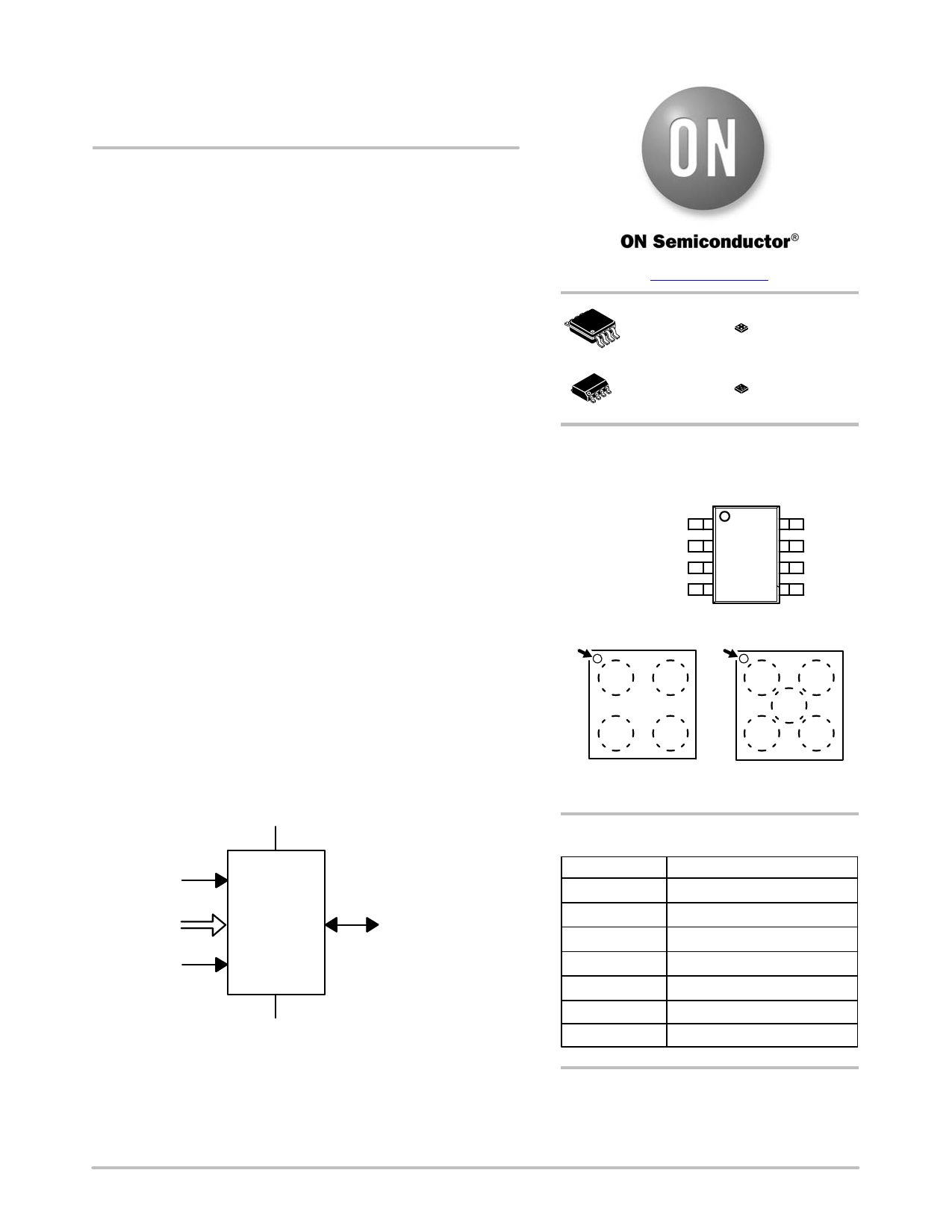
TSSOP−8
Y SUFFIX
CASE 948AL
SOIC−8
W SUFFIX
CASE 751BD
WLCSP−4***
C4A SUFFIX
CASE 567DC
WLCSP−5***
C5A SUFFIX
CASE 567DD
PIN CONFIGURATIONS
SOIC (W), TSSOP (Y)
CAV24C__
16 / 08 / 04 / 02
NC / NC / NC / A0
NC / NC / A1 / A1
NC / A2 / A2 / A2
VSS
1
8
2
7
3
6
4
5
Pin 1 1
(Top View)
2 Pin 1 1 2
VCC
WP
SCL
SDA
3
A VCC
VSS
B SCL SDA
VCC
VSS A
SDA
B
WP
SCL C
WLCSP−4***
WLCSP−5***
(Top Views)
PIN FUNCTION
Pin Name
A0, A1, A2
Function
Device Address Input
SDA
Serial Data Input/Output
SCL
Serial Clock Input
WP
Write Protect Input
VCC
Power Supply
VSS
Ground
NC
No Connect
ORDERING INFORMATION
See detailed ordering and shipping information in the package
dimensions section on page 10 of this data sheet.
© Semiconductor Components Industries, LLC, 2017
1
May, 2018 − Rev. 6
Publication Order Number:
CAV24C02/D
Share Link: 