BTS650PE3180A Ver la hoja de datos (PDF) - Siemens AG
Número de pieza
componentes Descripción
Fabricante
BTS650PE3180A Datasheet PDF : 16 Pages
| |||

Pin
1
2
3
4
5
6
7
BTS650P
Symbol
OUT
OUT
IN
Vbb
IS
OUT
OUT
Function
O
Output to the load. The pins 1,2,6 and 7 must be shorted with each other
especially in high current applications!3)
O Output to the load. The pins 1,2,6 and 7 must be shorted with each other
especially in high current applications!3)
I Input, activates the power switch in case of short to ground
+ Positive power supply voltage, the tab is electrically connected to this pin.
In high current applications the tab should be used for the Vbb connection
instead of this pin4).
S Diagnostic feedback providing a sense current proportional to the load
current; zero current on failure (see Truth Table on page 7)
O
Output to the load. The pins 1,2,6 and 7 must be shorted with each other
especially in high current applications!3)
O
Output to the load. The pins 1,2,6 and 7 must be shorted with each other
especially in high current applications!3)
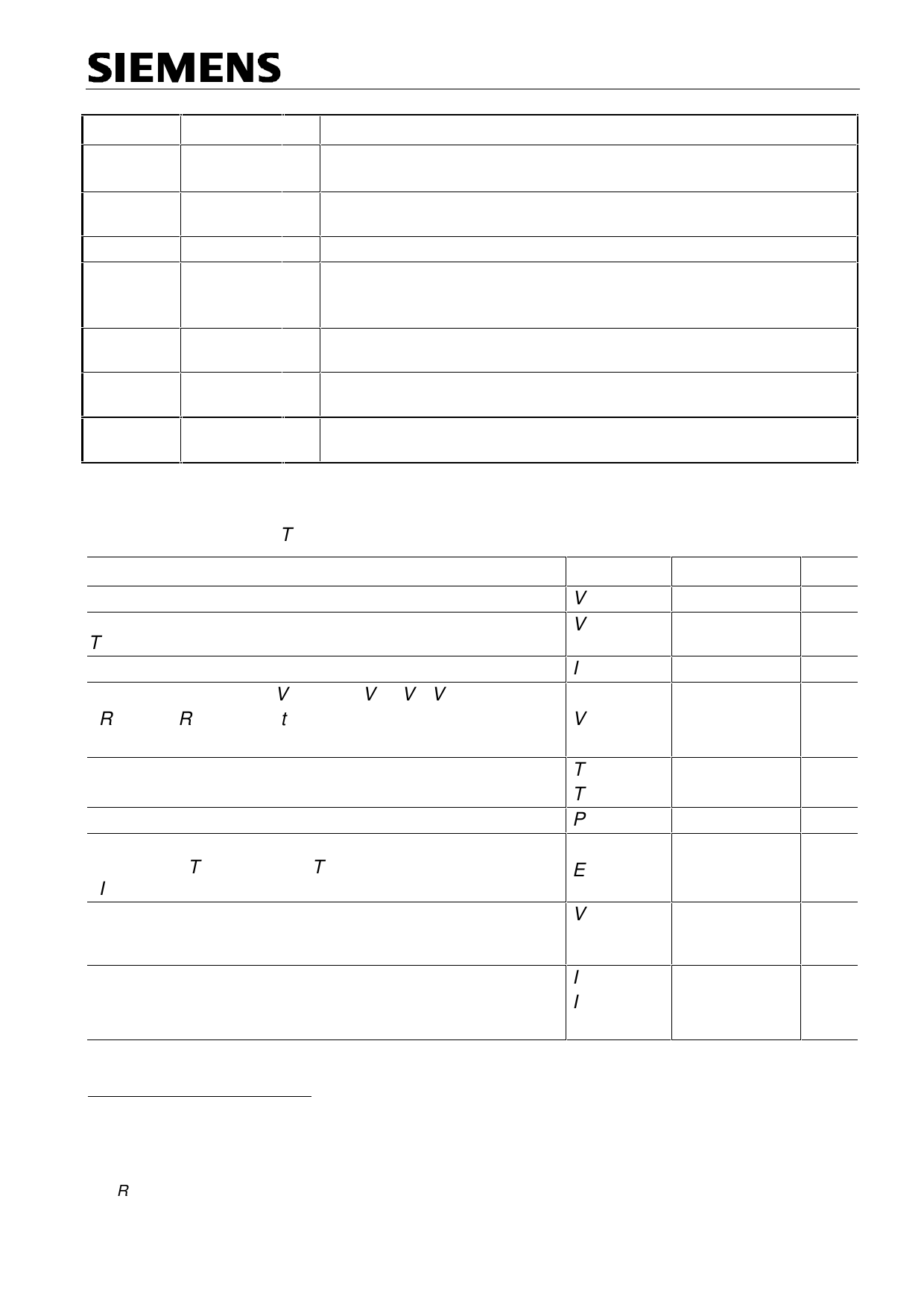
Maximum Ratings at Tj = 25 °C unless otherwise specified
Parameter
Supply voltage (overvoltage protection see page 4)
Supply voltage for short circuit protection,
Tj,start =-40 ...+150°C: (see diagram on page 10)
Load current (short circuit current, see page 5)
Load dump protection VLoadDump = VA + Vs, VA = 13.5 V
RI5) = 2 Ω, RL = 0.54 Ω, td = 200 ms,
IN, IS = open or grounded
Operating temperature range
Storage temperature range
Power dissipation (DC), TC ≤ 25 °C
Inductive load switch-off energy dissipation, single pulse
Vbb = 12V, Tj,start = 150°C, TC = 150°C const.,
IL = 20 A, ZL = 7.5 mH, 0 Ω, see diagrams on page 10
Electrostatic discharge capability (ESD)
Human Body Model acc. MIL-STD883D, method 3015.7 and ESD
assn. std. S5.1-1993, C = 100 pF, R = 1.5 kΩ
Current through input pin (DC)
Current through current sense status pin (DC)
see internal circuit diagrams on page 7 and 8
Symbol
Vbb
Vbb
IL
VLoad dump6)
Tj
Tstg
Ptot
EAS
VESD
IIN
IIS
Values Unit
42 V
34 V
self-limited A
75 V
-40 ...+150 °C
-55 ...+150
170 W
1.5
J
4 kV
+15 , -250 mA
+15 , -250
3) Not shorting all outputs will considerably increase the on-state resistance, reduce the peak current
capability and decrease the current sense accuracy
4) Otherwise add up to 0.7 mΩ (depending on used length of the pin) to the RON if the pin is used instead of
the tab.
5) RI = internal resistance of the load dump test pulse generator.
6) VLoad dump is setup without the DUT connected to the generator per ISO 7637-1 and DIN 40839.
Semiconductor Group
Page 2
1998-Nov.-2