ATT3042 Ver la hoja de datos (PDF) - Unspecified
Número de pieza
componentes Descripción
Fabricante
ATT3042 Datasheet PDF : 80 Pages
| |||
Data Sheet
February 1997
ATT3000 Series Field-Programmable Gate Arrays
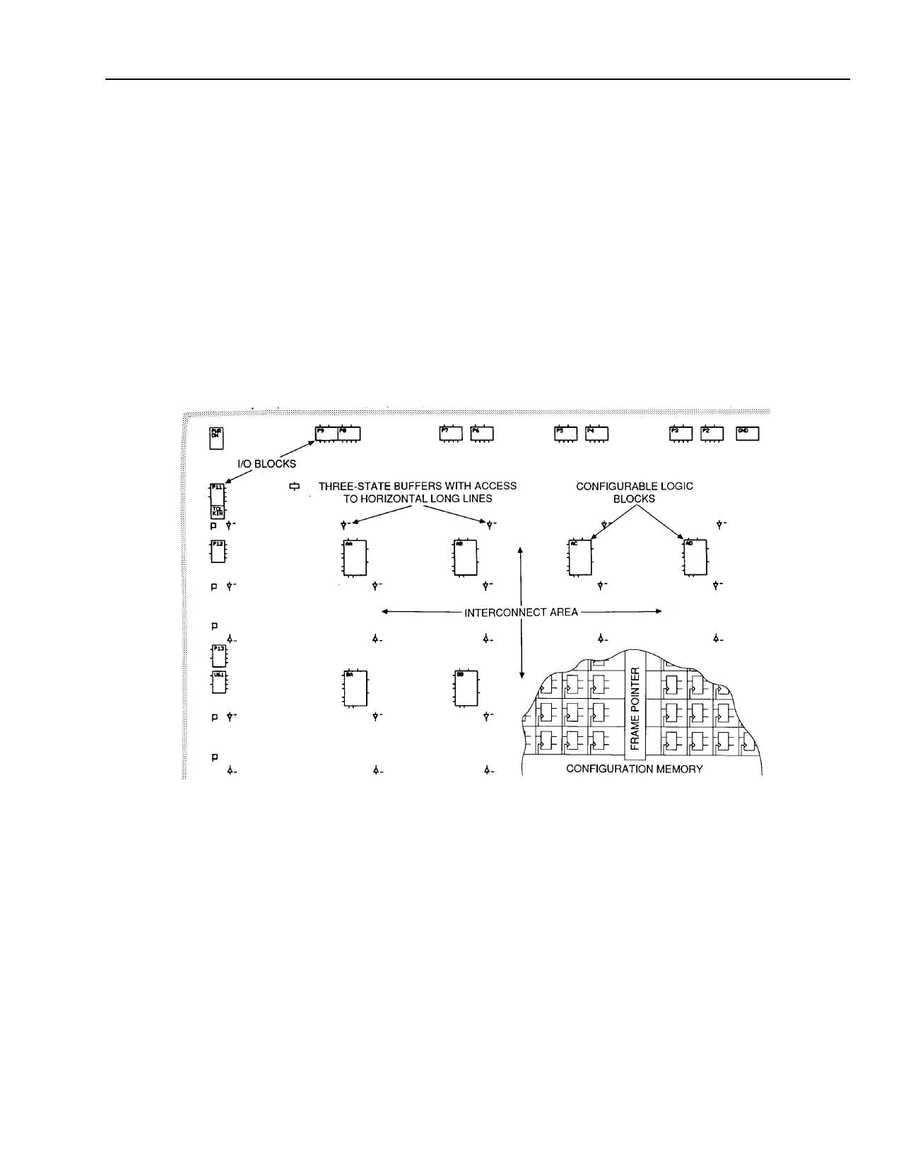
Architecture
The perimeter of configurable I/O blocks (IOBs) pro-
vides a programmable interface between the internal
logic array and the device package pins. The array of
configurable logic blocks (CLBs) performs user-
specified logic functions. The interconnect resources
are programmed to form networks, carrying logic
signals among blocks, analogous to printed-circuit
board traces connecting MSI/SSI packages.
The blocks’ logic functions are implemented by
programmed look-up tables. Functional options are
implemented by program-controlled multiplexers.
Interconnecting networks between blocks are
implemented with metal segments joined by program-
controlled pass transistors. These functions of the
FPGA are established by a configuration program
which is loaded into an internal, distributed array of
configuration memory cells. The configuration program
is loaded into the FPGA at powerup and may be
reloaded on command. The FPGA includes logic and
control signals to implement automatic or passive
configuration. Program data may be either bit serial or
byte parallel. The ORCA Foundry for ATT3000 Devel-
opment System generates the configuration program
bit stream used to configure the FPGA. The memory
loading process is independent of the user logic func-
tions.
Figure 1. Field-Programmable Gate Array Structure
Lucent Technologies Inc.
3
Share Link: 