AS28F128J3M Ver la hoja de datos (PDF) - Austin Semiconductor
Número de pieza
componentes Descripción
Fabricante
AS28F128J3M Datasheet PDF : 8 Pages
| |||
Austin Semiconductor, Inc.
PEM
AS28F128J3M
Q-Flash
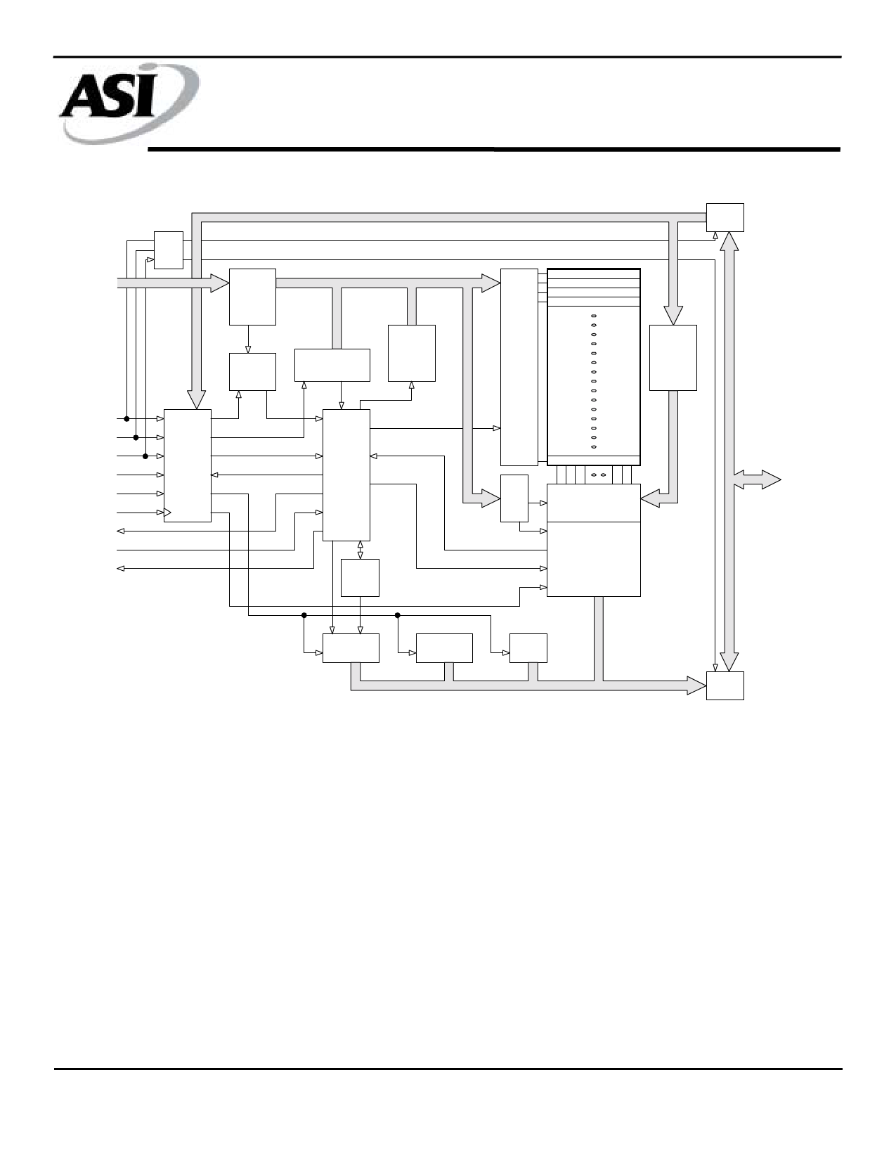
Functional Block Diagram:
CEx
OE\
WE\
RP\
WP\
CLK
STS
VPEN
WAIT
I/O
CNTL
Logic
ADDR
Buffer/
Latch
Power
(Current)
Control
Bus
Configuration
Register [BCR]
ADDR.
Counter
Command
Execution
Logic
ISM
[CEL]
VPP
Switch
Pump
Input
Buffer
X
Decode
128KB Memory Block (0)
128KB Memory Block (1)
128KB Memory Block (2)
128KB Memory Block (3)
Block
Erase
Control
WRITE
Buffer
128KB Memory Block (n)
Y
Dec.
Y - Select
Control
Sense Amplifiers
WRITE/ERASE Bit
Compare and
Verify
DQ0-8 or
DQ0-15
Status
Register
Identification
Register
Query
Output
Buffer
Additionally, the Scaleable Command Set [SCS] allows a single,
simple software driver in all host systems to work with all SCS VPEN serves as an input with 2.7V, 3.3V or 5V levels for
compliant FLASH memory devices. The SCS provides the fastest application programming. VPEN in this Q-Flash device can
system/device data transfer rates and minimizes the device and provide data protection when connected to ground. This pin also
system-level implementation costs.
enables PROGRAM or ERASE LOCKOUT functions/controls
during power transitions.
To optimize the processor-memory interface, the device
accommodates VPEN, which is switchable during BLOCK This device is an even-sectored device architecture offering
ERASE, PROGRAM, or LOCK BIT configurations and in individual BLOCK LOCKING that can LOCK and UN-LOCK a
addition can be hard-wired to VCC all dependent on the end block using the SECTOR LOCK BITS command sequence.
application(s). VPEN is treated as an input pin to enable
ERASING, PROGRAMMING, and BLOCK LOCKING. When Status [STS] is a logic signal output that gives an additional
VPEN is lower than the VCC lockout voltage (VLKO), all indicator of the internal state machine [ISM] activity by providing
program functions are disabled. BLOCK ERASE SUSPEND a hardware signal of both the status and status masking. This
mode enables the user to stop BLOCK ERASE to READ data status indicator minimizes central processing unit overhead and
from or PROGRAM data to any other blocks. Similarly, system power consumption. In the default mode, STS acts as an
PROGRAM SUSPEND mode enables the user to SUSPEND RY/BY\ pin. When LOW, STS indicates that the ISM is
PROGRAMMING to READ data or execute code from any un- performing a BLOCK ERASE, PROGRAM, or LOCK BIT
suspended block(s).
configuration. When HIGH, STS indicates that the ISM is ready
for a new command.
AS28F128J3MRG
Revision 5.0 11/23/04
Austin Semiconductor, Inc. reserves the right to change products or modify product specifications with appropriate notification
For Additional Products and Information visit out Web site at www.austinsemiconductor.com
2
Share Link: 