APT8020JFLL Ver la hoja de datos (PDF) - Microsemi Corporation
NГәmero de pieza
componentes DescripciГіn
Fabricante
APT8020JFLL Datasheet PDF : 5 Pages
| |||
DYNAMIC CHARACTERISTICS
APT8020JFLL
Symbol Characteristic
Test Conditions
MIN TYP MAX UNIT
Ciss
Coss
Crss
Input Capacitance
Output Capacitance
Reverse Transfer Capacitance
VGS = 0V
VDS = 25V
f = 1 MHz
5200
1000
pF
190
Qg
Total Gate Charge 3
Qgs Gate-Source Charge
Qgd Gate-Drain ("Miller") Charge
VGS = 10V
VDD = 400V
ID = 33A @ 25В°C
195
27
nC
130
td(on)
tr
td(off)
tf
Eon
Eoff
Eon
Eoff
Turn-on Delay Time
Rise Time
Turn-off Delay Time
Fall Time
Turn-on Switching Energy 6
Turn-off Switching Energy
Turn-on Switching Energy 6
Turn-off Switching Energy
RESISTIVE SWITCHING
12
VGS = 15V
VDD = 400V
ID = 33A @ 25В°C
14
ns
39
RG = 0.6в„Ұ
10
INDUCTIVE SWITCHING @ 25В°C
VDD = 533V, VGS = 15V
760
ID = 33A, RG = 5в„Ұ
715
ВөJ
INDUCTIVE SWITCHING @ 125В°C
1250
VDD = 533V, VGS = 15V
ID = 33A, RG = 5в„Ұ
780
SOURCE-DRAIN DIODE RATINGS AND CHARACTERISTICS
Symbol Characteristic / Test Conditions
MIN TYP MAX UNIT
IS
Continuous Source Current (Body Diode)
ISM Pulsed Source Current 1 (Body Diode)
33 Amps
132
VSD Diode Forward Voltage 2 (VGS = 0V, IS = -33A)
dv/dt
Peak Diode Recovery dv/dt 5
1.3 Volts
18 V/ns
trr
Reverse Recovery Time
(IS = -33A, di/dt = 100A/Вөs)
Tj = 25В°C
Tj = 125В°C
320
ns
650
Reverse Recovery Charge
Qrr
(IS = -33A, di/dt = 100A/Вөs)
Tj = 25В°C
Tj = 125В°C
1.4
ВөC
5.9
Peak Recovery Current
IRRM
(IS = -33A, di/dt = 100A/Вөs)
Tj = 25В°C
Tj = 125В°C
10.8
Amps
18.9
THERMAL CHARACTERISTICS
Symbol Characteristic
MIN TYP MAX UNIT
RОёJC
RОёJA
Junction to Case
Junction to Ambient
0.24
40
В°C/W
1 Repetitive Rating: Pulse width limited by maximum junction
temperature
2 Pulse Test: Pulse width < 380 Вөs, Duty Cycle < 2%
3 See MIL-STD-750 Method 3471
4 Starting Tj = +25В°C, L = 5.51mH, RG = 25в„Ұ, Peak IL = 33A
5 dv/dt numbers reflect the limitations of the test circuit rather than the
device itself. IS вүӨ -ID33A di/dt вүӨ 700A/Вөs VR вүӨ 800V TJ вүӨ 150В°C
6 Eon includes diode reverse recovery. See figures 18, 20.
Microsemi reserves the right to change, without notice, the specifications and inforation contained herein.
0.25
0.9
0.20
0.7
0.15
0.10
0.05
0
10-5
0.5
Note:
0.3
0.1
0.05
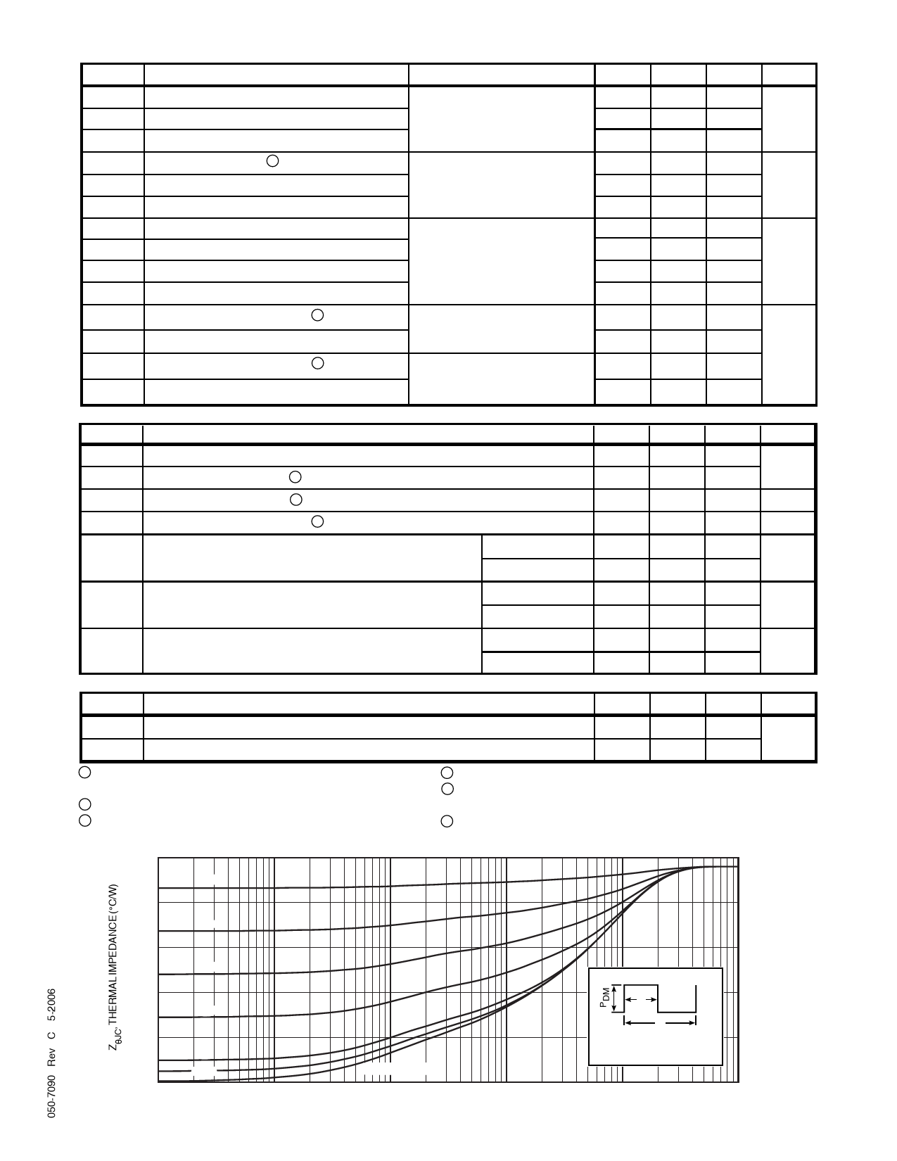
SINGLE PULSE
t1
t2
Duty Factor D = t1/t2
Peak TJ = PDM x ZОёJC + TC
10-4
10-3
10-2
10-1
1.0
RECTANGULAR PULSE DURATION (SECONDS)
FIGURE 1, MAXIMUM EFFECTIVE TRANSIENT THERMAL IMPEDANCE, JUNCTION-TO-CASE vs PULSE DURATION
Share Link: 