ADSP-2186L1111 Ver la hoja de datos (PDF) - Analog Devices
Número de pieza
componentes Descripción
Fabricante
ADSP-2186L1111 Datasheet PDF : 36 Pages
| |||
ADSP-2186L
There are 8160 words of memory accessible internally when the
DMOVLAY register is set to 0. When DMOVLAY is set to
something other than 0, external accesses occur at addresses
0x0000 through 0x1FFF. The external address is generated as
shown in Table III.
Table III. DMOVLAY Addressing
DMOVLAY Memory A13
A12:0
0
Internal Not Applicable Not Applicable
1
External
Overlay 1 0
13 LSBs of Address
Between 0x0000
and 0x1FFF
2
External
Overlay 2 1
13 LSBs of Address
Between 0x0000
and 0x1FFF
This organization allows for two external 8K overlays using only
the normal 14 address bits. All internal accesses complete in one
cycle. Accesses to external memory are timed using the wait
states specified by the DWAIT register.
I/O Space (Full Memory Mode)
The ADSP-2186L supports an additional external memory
space called I/O space. This space is designed to support simple
connections to peripherals or to bus interface ASIC data regis-
ters. I/O space supports 2048 locations. The lower eleven bits
of the external address bus are used; the upper three bits are
undefined. Two instructions were added to the core ADSP-
2100 Family instruction set to read from and write to I/O
memory space. The I/O space also has four dedicated three-bit
wait state registers, IOWAIT0-3, that specify up to seven wait
states to be automatically generated for each of four regions.
The wait states act on address ranges as shown in Table IV.
Table IV.
Address Range
0x000–0x1FF
0x200–0x3FF
0x400–0x5FF
0x600–0x7FF
Wait State Register
IOWAIT0
IOWAIT1
IOWAIT2
IOWAIT3
Composite Memory Select (CMS)
The ADSP-2186L has a programmable memory select signal
that is useful for generating memory select signals for memories
mapped to more than one space. The CMS signal is generated
to have the same timing as each of the individual memory select
signals (PMS, DMS, BMS, IOMS), but can combine their
functionality.
Each bit in the CMSSEL register, when set, causes the CMS
signal to be asserted when the selected memory select is asserted.
For example, to use a 32K word memory to act as both program
and data memory, set the PMS and DMS bits in the CMSSEL
register and use the CMS pin to drive the chip select of the
memory and use either DMS or PMS as the additional address bit.
The CMS pin functions as the other memory select signal, with
the same timing and bus request logic. A 1 in the enable bit
causes the assertion of the CMS signal at the same time as the
selected memory select signal. All enable bits, except the BMS
bit, default to 1 at reset.
Boot Memory Select (BMS) Disable
The ADSP-2186L also lets you boot the processor from one
external memory space while using a different external memory
space for BDMA transfers during normal operation. You can
use the CMS to select the first external memory space for BDMA
transfers and BMS to select the second external memory space
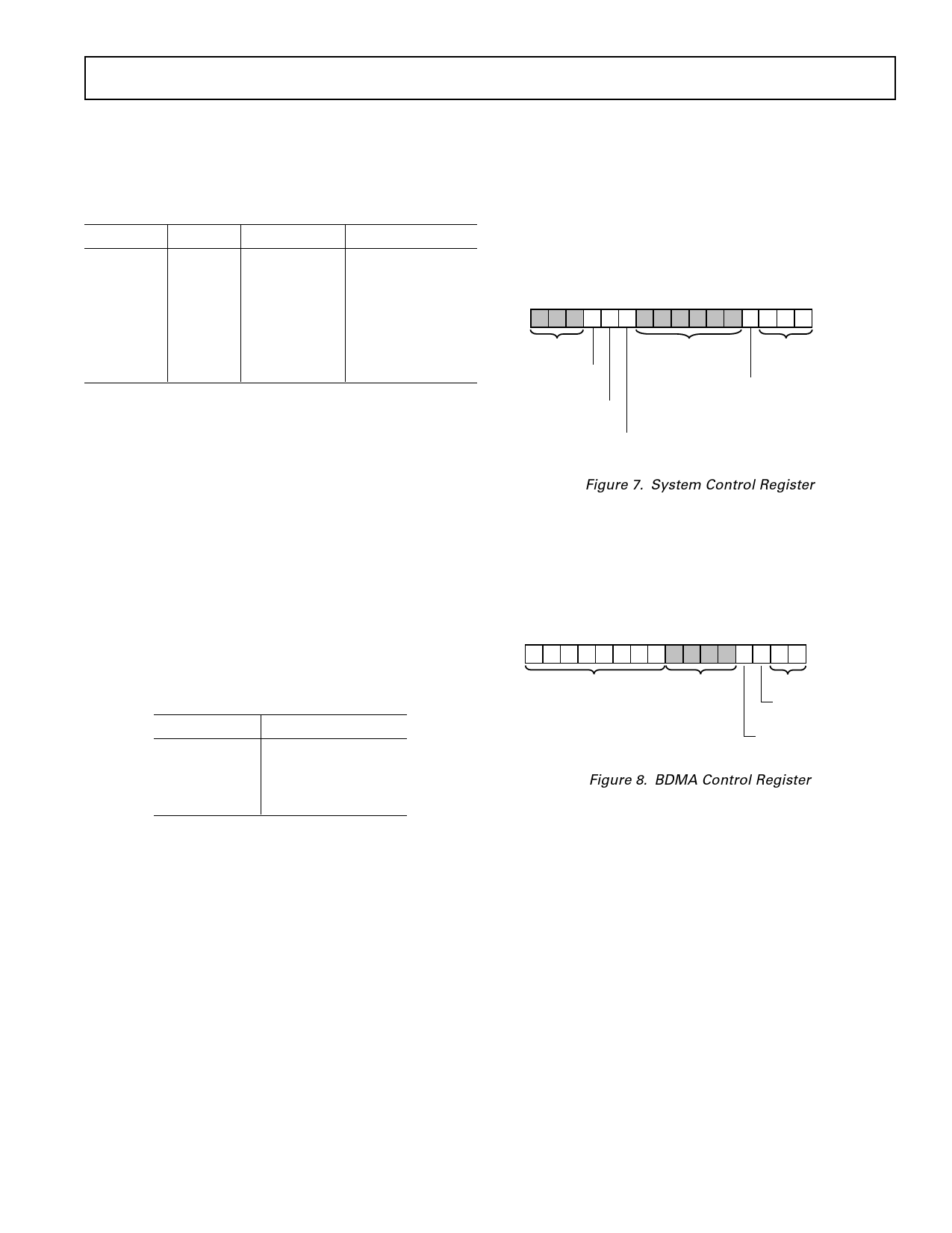
for booting. The BMS signal can be disabled by setting Bit 3 of
the System Control Register to 1. The System Control Register
is illustrated in Figure 7.
SYSTEM CONTROL REGISTER
15 14 13 12 11 10 9 8 7 6 5 4 3 2 1 0
0 0 0 0 0 1 0 0 0 0 0 0 0 1 1 1 DM(0x3FFF)
RESERVED
SET TO 0
RESERVED SET TO 0
PWAIT
PROGRAM MEMORY
SPORT0 ENABLE
WAIT STATES
1 = ENABLED
0 = DISABLED
SPORT1 ENABLE
BMS ENABLE
0 = ENABLED
1 = DISABLED
1 = ENABLED
0 = DISABLED
SPORT1 CONFIGURE
1 = SERIAL PORT
0 = FI, FO, IRQ0, IRQ1, SCLK
Figure 7. System Control Register
Byte Memory
The byte memory space is a bidirectional, 8-bit-wide, external
memory space used to store programs and data. Byte memory is
accessed using the BDMA feature. The BDMA Control Register is
shown in Figure 8. The byte memory space consists of 256 pages,
each of which is 16K × 8.
BDMA CONTROL
15 14 13 12 11 10 9 8 7 6 5 4 3 2 1 0
0 0 0 0 0 0 0 0 0 0 0 0 1 0 0 0 DM (0؋3FE3)
BMPAGE
RESERVED
SET TO ZERO
BTYPE
BDIR
0 = LOAD FROM BM
1 = STORE TO BM
BCR
0 = RUN DURING BDMA
1 = HALT DURING BDMA
Figure 8. BDMA Control Register
The byte memory space on the ADSP-2186L supports read and
write operations as well as four different data formats. The byte
memory uses data bits 15:8 for data. The byte memory uses
data bits 23:16 and address bits 13:0 to create a 22-bit address.
This allows up to a 4 meg × 8 (32 megabit) ROM or RAM to be
used without glue logic. All byte memory accesses are timed by
the BMWAIT register.
Byte Memory DMA (BDMA, Full Memory Mode)
The byte memory DMA controller allows loading and storing of
program instructions and data using the byte memory space.
The BDMA circuit is able to access the byte memory space
while the processor is operating normally and steals only one
DSP cycle per 8-, 16- or 24-bit word transferred.
The BDMA circuit supports four different data formats, that are
selected by the BTYPE register field. The appropriate number
of 8-bit accesses is determined from the byte memory space to
build the word size selected. Table V shows the data formats sup-
ported by the BDMA circuit.
REV. B
–9–
Share Link: 