ADP5020(RevA) Ver la hoja de datos (PDF) - Analog Devices
Número de pieza
componentes Descripción
Fabricante
ADP5020 Datasheet PDF : 28 Pages
| |||
Data Sheet
ADP5020
I2C TIMING SPECIFICATIONS
Table 6.
Parameter
fSCL
tHIGH
tLOW
tSU,DAT
tHD,DAT1
tSU,STA
tHD,STA
tBUF
tSU,STO
tRISE
tFALL
tSP
CB2
Min
Max
400
0.6
1.3
100
0
0.9
0.6
0.6
1.3
0.6
20 + 0.1CB
300
20 + 0.1CB
300
0
50
400
Unit Description
kHz
SCL clock frequency
μs
SCL high time
μs
SCL low time
ns
Data setup time
μs
Data hold time
μs
Setup time for repeated start
μs
Hold time for start/repeated start
μs
Bus free time between a stop condition and a start condition
μs
Setup time for stop condition
ns
Rise time of SCL/SDA
ns
Fall time of SCL/SDA
ns
Pulse width of suppressed spike
pF
Capacitive load for each bus line
1 A master device must provide a hold time of at least 300 ns for the SDA signal (referred to the VIHMIN of the SCL signal) to bridge the undefined region of the SCL falling edge.
2 CB is the total capacitance of one bus line in picofarads (pF).
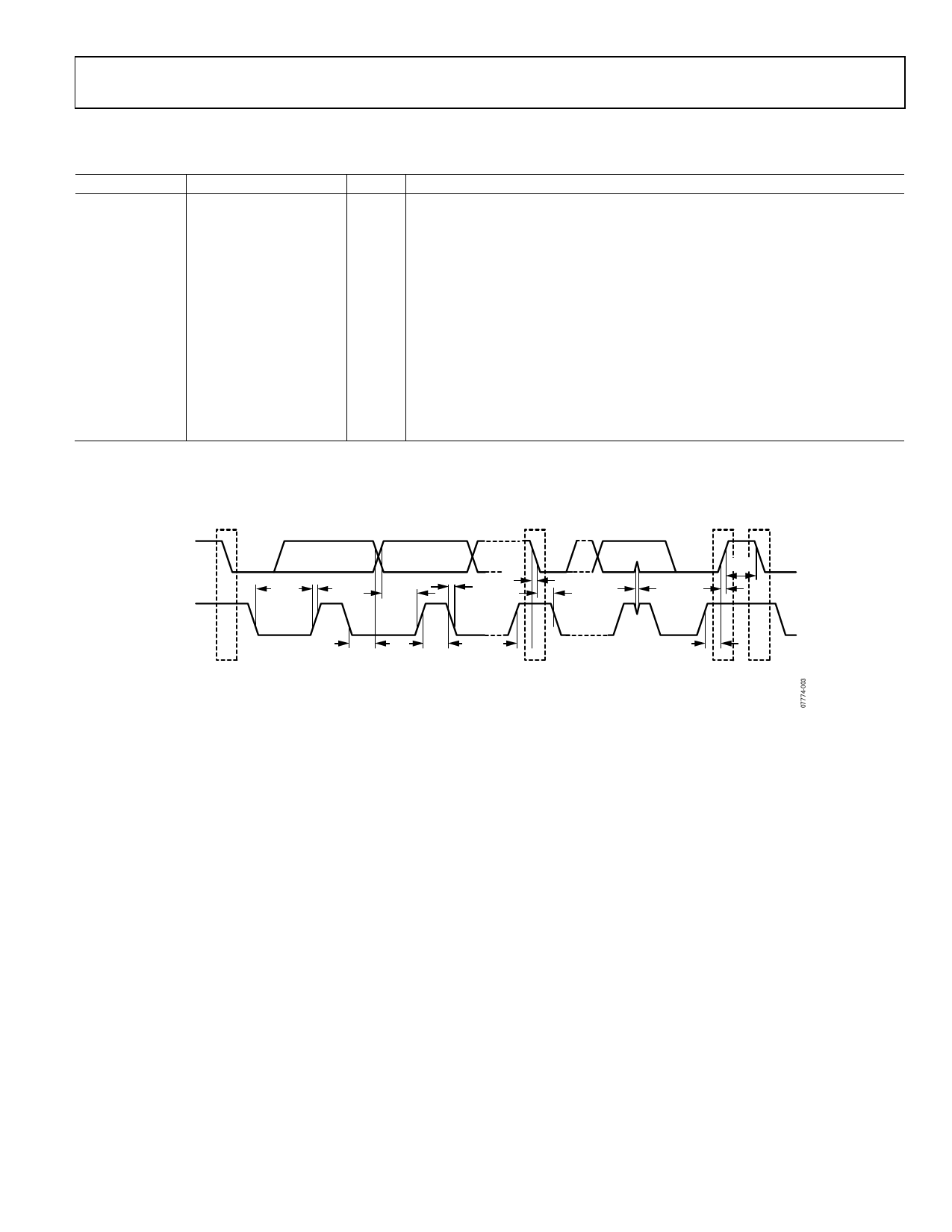
Timing Diagram
SDA
tLOW
tRISE
SCL
S
tHD,DAT
S = START CONDITION
Sr = START REPEATED CONDITION
P = STOP CONDITION
tSU,DAT
tFALL
tFALL
tHD,STA
tHIGH
tSU,STA
Sr
Figure 3. I2C Interface Timing Diagram
tSP tRISE
tBUF
tSU,STO
P
S
Rev. A | Page 7 of 28
Share Link: 