ADN4667 Ver la hoja de datos (PDF) - Analog Devices
Número de pieza
componentes Descripción
Fabricante
ADN4667 Datasheet PDF : 16 Pages
| |||
ADN4667
Data Sheet
AC CHARACTERISTICS
VCC = 3.0 V to 3.6 V; RL = 100 Ω; CL1 = 15 pF to GND; all specifications TMIN to TMAX, unless otherwise noted. All typical values are given
for VCC = +3.3 V, TA = +25°C.
Table 2.
Parameter2
Min Typ
Differential Propagation Delay, High to Low, tPHLD 0.5
0.9
Differential Propagation Delay, Low to High, tPLHD 0.5
1.2
Differential Pulse Skew |tPHLD − tPLHD|, tSKD15
0
0.3
Channel-to-Channel Skew, tSKD26
0
0.4
Differential Part-to-Part Skew, tSKD37
0
Differential Part-to-Part Skew, tSKD48
0
Rise Time, tr
0.5
Fall Time, tf
0.5
Disable Time High to Inactive, tPHZ
2
Disable Time Low to Inactive, tPLZ
2
Enable Time Inactive to High, tPZH
3
Enable Time Inactive to Low, tPZL
3
Maximum Operating Frequency, fMAX9
200 250
Max Unit
1.7 ns
1.7 ns
0.4 ns
0.5 ns
1.0 ns
1.2 ns
1.5 ns
1.5 ns
5
ns
5
ns
7
ns
7
ns
MHz
Conditions/Comments3, 4
See Figure 3 and Figure 4
See Figure 3 and Figure 4
See Figure 3 and Figure 4
See Figure 3 and Figure 4
See Figure 3 and Figure 4
See Figure 3 and Figure 4
See Figure 3 and Figure 4
See Figure 3 and Figure 4
See Figure 5 and Figure 6
See Figure 5 and Figure 6
See Figure 5 and Figure 6
See Figure 5 and Figure 6
See Figure 5 and Figure 6
1 CL includes probe and jig capacitance.
2 AC parameters are guaranteed by design and characterization.
3 Generator waveform for all tests unless otherwise specified: f = 50 MHz, ZO = 50 Ω, tr ≤ 1 ns, and tf ≤ 1 ns.
4 All input voltages are for one channel unless otherwise specified. Other inputs are set to GND.
5 tSKD1 = |tPHLD − tPLHD| is the magnitude difference in differential propagation delay time between the positive going edge and the negative going edge of the
same channel.
6 tSKD2 is the differential channel-to-channel skew of any event on the same device.
7 tSKD3, differential part-to-part skew, is defined as the difference between the minimum and maximum specified differential propagation delays. This specification
applies to devices at the same VCC and within 5°C of each other within the operating temperature range.
8 tSKD4, part-to-part skew, is the differential channel-to-channel skew of any event between devices. This specification applies to devices over recommended operating
temperatures and voltage ranges, and across process distribution. tSKD4 is defined as |maximum − minimum| differential propagation delay.
9 fMAX generator input conditions: tr = tf < 1 ns (0% to 100%), 50% duty cycle, 0 V to 3 V. Output criteria: duty cycle = 45% to 55%, VOD > 250 mV, all channels switching.
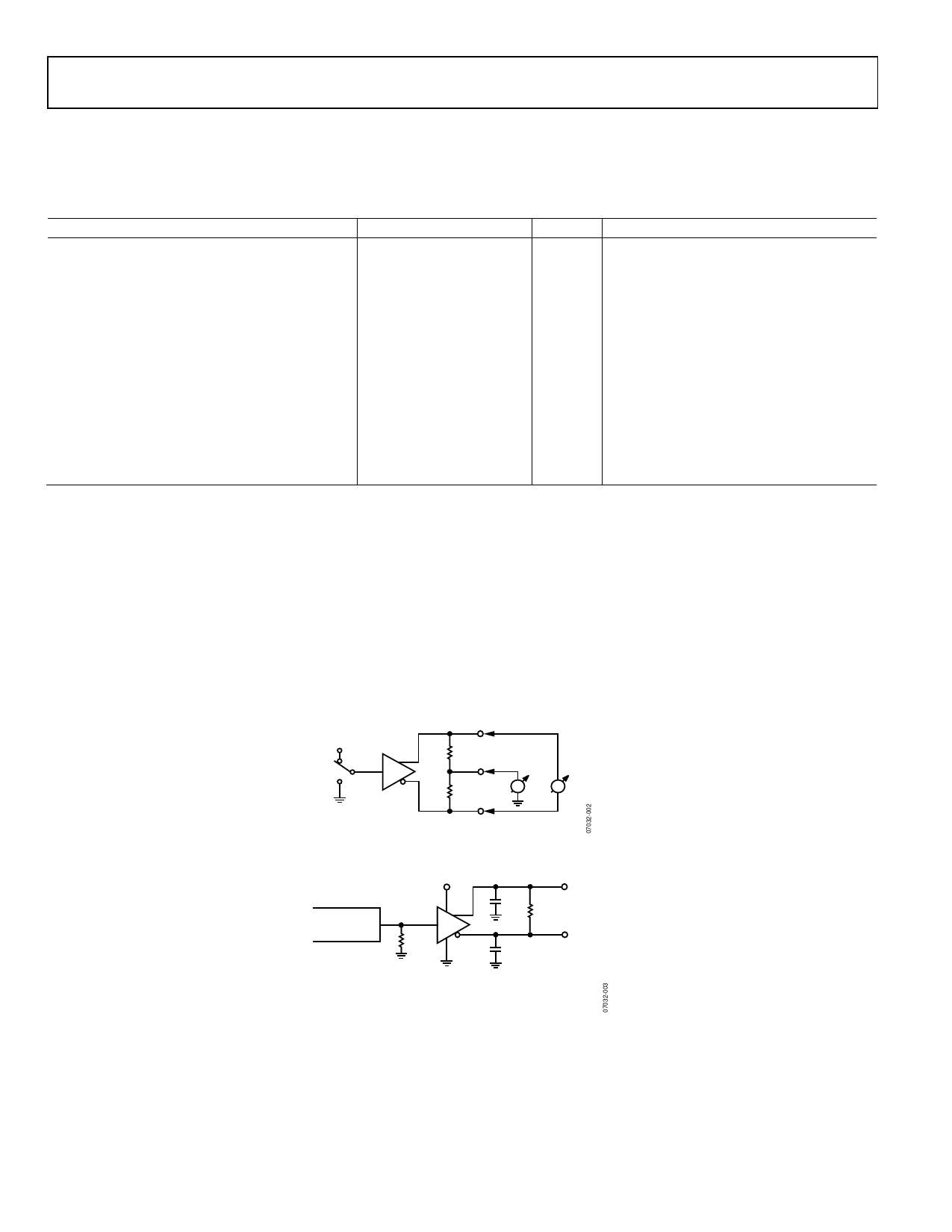
Test Circuits and Timing Diagrams
VCC
DIN
DOUT+
RL/2
RL/2
V VOS V VOD
DRIVER IS ENABLED
DOUT–
Figure 2. Test Circuit for Driver VOD and VOS
VCC
CL
SIGNAL
DIN
GENERATOR
50Ω
CL
DOUT+
DOUT–
DRIVER IS
ENABLED
NOTES
1. CL INCLUDES LOAD AND TEST JIG CAPACITANCE.
Figure 3. Test Circuit for Driver Propagation Delay and Transition Time
Rev. B | Page 4 of 16
Share Link: 