ADG758BCP Ver la hoja de datos (PDF) - Analog Devices
Número de pieza
componentes Descripción
Fabricante
ADG758BCP Datasheet PDF : 12 Pages
| |||
ADG758/ADG759
ABSOLUTE MAXIMUM RATINGS1
(TA = 25°C, unless otherwise noted.)
VDD to VSS . . . . . . . . . . . . . . . . . . . . . . . . . . . . . . . . . . . . . 7 V
VDD to GND . . . . . . . . . . . . . . . . . . . . . . . . . . –0.3 V to +7 V
VSS to GND . . . . . . . . . . . . . . . . . . . . . . . . . . +0.3 V to –3.5 V
Analog Inputs2 . . . . . . . . . . . . . . VSS – 0.3 V to VDD +0.3 V or
30 mA, Whichever Occurs First
Digital Inputs2 . . . . . . . . . . . . . . . . . . –0.3 V to VDD +0.3 V or
30 mA, Whichever Occurs First
Peak Current, S or D . . . . . . . . . . . . . . . . . . . . . . . . . . 100 mA
(Pulsed at 1 ms, 10% Duty Cycle max)
Continuous Current, S or D . . . . . . . . . . . . . . . . . . . . . 30 mA
Operating Temperature Range
Industrial (B Version) . . . . . . . . . . . . . . . . –40°C to +85°C
Storage Temperature Range . . . . . . . . . . . . –65°C to +150°C
Junction Temperature . . . . . . . . . . . . . . . . . . . . . . . . . . 150°C
Chip Scale Package,
θJA Thermal Impedance . . . . . . . . . . . . . . . . . . . . . . 32°C/W
Lead Temperature, Soldering
Vapor Phase (60 sec) . . . . . . . . . . . . . . . . . . . . . . . . . 215°C
Infrared (15 sec) . . . . . . . . . . . . . . . . . . . . . . . . . . . . . 220°C
NOTES
1Stresses above those listed under Absolute Maximum Ratings may cause perma-
nent damage to the device. This is a stress rating only; functional operation of the
device at these or any other conditions above those listed in the operational
sections of this specification is not implied. Exposure to absolute maximum rating
conditions for extended periods may affect device reliability. Only one absolute
maximum rating may be applied at any one time.
2Overvoltages at EN, A, S, or D will be clamped by internal diodes. Current should
be limited to the maximum ratings given.
CAUTION
ESD (electrostatic discharge) sensitive device. Electrostatic charges as high as 4000 V readily
accumulate on the human body and test equipment and can discharge without detection. Although
the ADG758/ADG759 features proprietary ESD protection circuitry, permanent damage may
occur on devices subjected to high-energy electrostatic discharges. Therefore, proper ESD
precautions are recommended to avoid performance degradation or loss of functionality.
WARNING!
ESD SENSITIVE DEVICE
Table I. ADG758 Truth Table
A2
A1
A0
X
X
X
0
0
0
0
0
1
0
1
0
0
1
1
1
0
0
1
0
1
1
1
0
1
1
1
X = Don’t Care
EN
Switch Condition
0
NONE
1
1
1
2
1
3
1
4
1
5
1
6
1
7
1
8
Table II. ADG759 Truth Table
A1
A0
X
X
0
0
0
1
1
0
1
1
X = Don’t Care
EN
ON Switch Pair
0
NONE
1
1
1
2
1
3
1
4
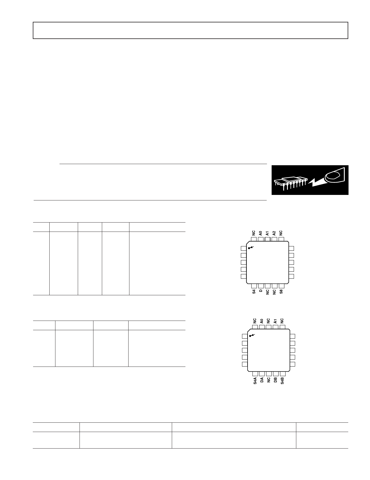
PIN CONFIGURATIONS
EN 1
VSS 2
S1 3
S2 4
S3 5
20 19 18 17 16
PIN 1
IDENTIFIER
ADG758
TOP VIEW
(Not to Scale)
15 GND
14 VDD
13 S5
12 S6
11 S7
6 7 8 9 10
NC = NO CONNECT
EXPOSED PAD TIED TO SUBSTRATE, VSS
EN 1
VSS 2
S1A 3
S2A 4
S3A 5
20 19 18 17 16
PIN 1
IDENTIFIER
ADG759
TOP VIEW
(Not to Scale)
15 GND
14 VDD
13 S1B
12 S2B
11 S3B
6 7 8 9 10
NC = NO CONNECT
EXPOSED PAD TIED TO SUBSTRATE, VSS
Model
ADG758BCP
ADG759BCP
Temperature Range
–40°C to +85°C
–40°C to +85°C
ORDERING GUIDE
Package Description
20-Lead Chip Scale Package (CSP)
20-Lead Chip Scale Package (CSP)
Package Option
CP-20
CP-20
REV. A
–5–
Share Link: 