ADG758BCP Ver la hoja de datos (PDF) - Analog Devices
Número de pieza
componentes Descripción
Fabricante
ADG758BCP Datasheet PDF : 12 Pages
| |||
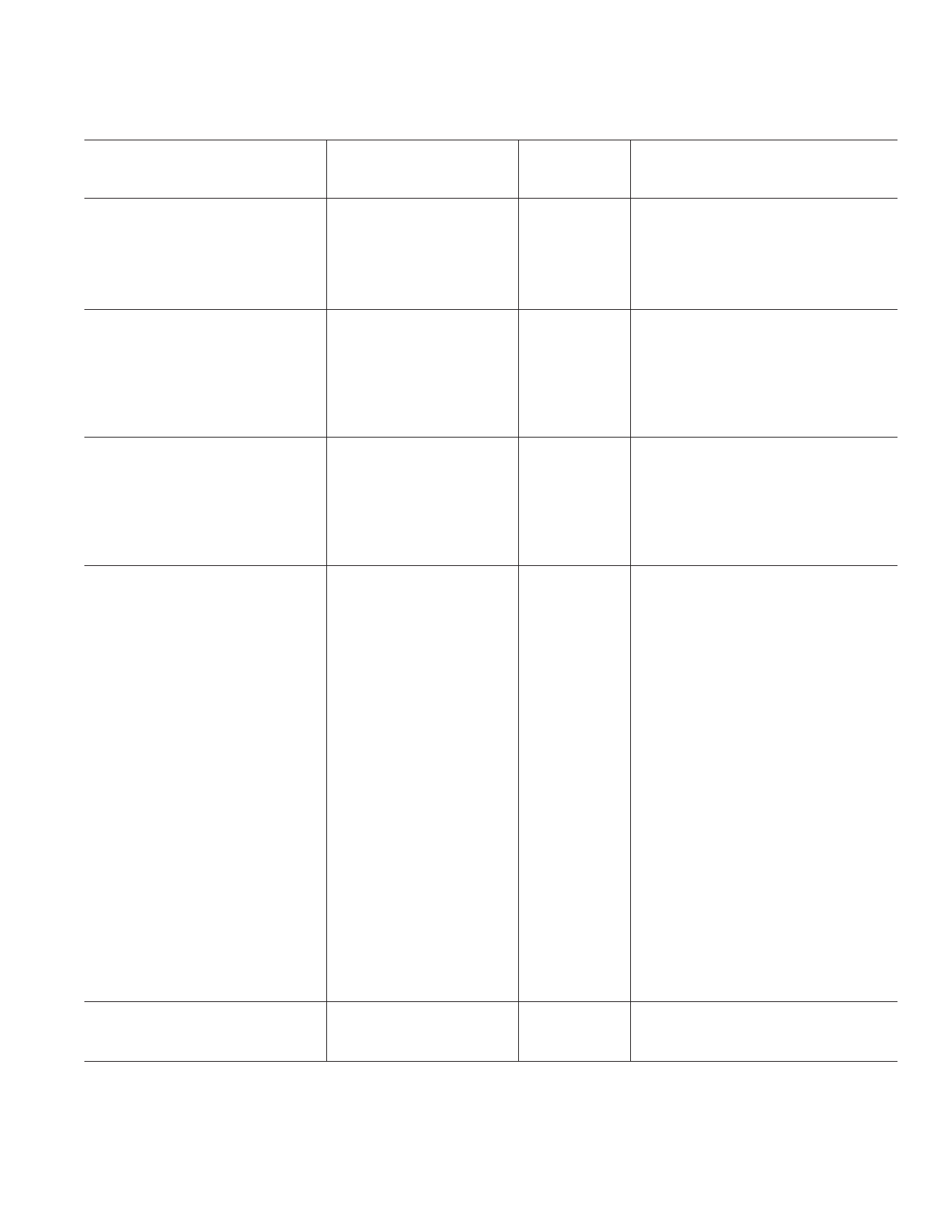
SPECIFICATIONS1
(VDD = 3 V ؎ 10%, VSS = 0 V, GND = 0 V, unless otherwise noted.)
ADG758/ADG759
Parameter
B Version
–40؇C
+25؇C
to +85؇C
Unit
Test Conditions/Comments
ANALOG SWITCH
Analog Signal Range
ON Resistance (RON)
ON Resistance Match Between
Channels (∆RON)
LEAKAGE CURRENTS
Source OFF Leakage IS (OFF)
Drain OFF Leakage ID (OFF)
Channel ON Leakage ID, IS (ON)
8
11
± 0.01
± 0.1
± 0.01
± 0.1
± 0.01
± 0.1
0 V to VDD
12
0.4
1.2
± 0.3
± 0.75
± 0.75
V
Ω typ
Ω max
Ω typ
Ω max
nA typ
nA max
nA typ
nA max
nA typ
nA max
VS = 0 V to VDD, IDS = 10 mA;
Test Circuit 1
VS = 0 V to VDD, IDS = 10 mA
VDD = 3.3 V
VS = 3 V/1 V, VD = 1 V/3 V;
Test Circuit 2
VS = 3 V/1 V, VD = 1 V/3 V;
Test Circuit 3
VS = VD = 1 V or 3 V; Test Circuit 4
DIGITAL INPUTS
Input High Voltage, VINH
Input Low Voltage, VINL
Input Current
IINL or IINH
CIN, Digital Input Capacitance
DYNAMIC CHARACTERISTICS2
tTRANSITION
Break-Before-Make Time Delay, tD
tON (EN)
tOFF (EN)
Charge Injection
Off Isolation
Channel-to-Channel Crosstalk
–3 dB Bandwidth
CS (OFF)
CD (OFF)
ADG758
ADG759
CD, CS (ON)
ADG758
ADG759
0.005
2
18
8
18
8
±3
–60
–80
–60
–80
55
13
85
42
96
48
2.0
0.8
± 0.1
30
1
30
15
V min
V max
µA typ
µA max
pF typ
ns typ
ns max
ns typ
ns min
ns typ
ns max
ns typ
ns max
pC typ
dB typ
dB typ
dB typ
dB typ
MHz typ
pF typ
pF typ
pF typ
pF typ
pF typ
VIN = VINL or VINH
RL = 300 Ω, CL = 35 pF; Test Circuit 5
VS1 = 2 V/0 V, VS2 = 0 V/2 V
RL = 300 Ω, CL = 35 pF
VS = 2 V; Test Circuit 6
RL = 300 Ω, CL = 35 pF
VS = 2 V; Test Circuit 7
RL = 300 Ω, CL = 35 pF
VS = 2 V; Test Circuit 7
VS = 1.5 V, RS = 0 Ω, CL = 1 nF;
Test Circuit 8
RL = 50 Ω, CL = 5 pF, f = 10 MHz
RL = 50 Ω, CL = 5 pF, f = 1 MHz;
Test Circuit 9
RL = 50 Ω, CL = 5 pF, f = 10 MHz
RL = 50 Ω, CL = 5 pF, f = 1 MHz;
Test Circuit 10
RL = 50 Ω, CL = 5 pF; Test Circuit 11
f = 1 MHz
f = 1 MHz
f = 1 MHz
f = 1 MHz
f = 1 MHz
POWER REQUIREMENTS
IDD
0.001
1.0
µA typ
µA max
VDD = 3.3 V
Digital Inputs = 0 V or 3.3 V
NOTES
1Temperature ranges are as follows: B Version: –40°C to +85°C.
2Guaranteed by design, not subject to production test.
Specifications subject to change without notice.
REV. A
–3–
Share Link: 