AD28MSP01 Ver la hoja de datos (PDF) - Analog Devices
Número de pieza
componentes Descripción
Fabricante
AD28MSP01 Datasheet PDF : 28 Pages
| |||
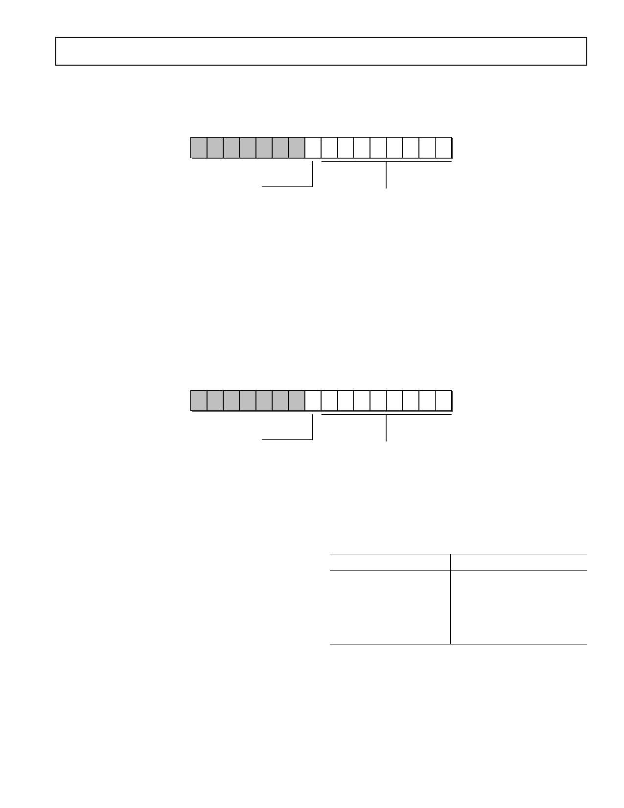
Control Register 4
address = 0x04
This register is the Receive Phase Adjust Register and it is used to:
• Change the phase of the receive clocks (RBAUD, RBIT, RCONV)
15 14 13 12 11 10 9 8 7 6 5 4 3 2 1 0
0 00 0 0 00 0 00 00 0 000
AD28msp01
0 – Phase advance
1 – Phase retard
P7-0
Phase Shift Magnitude
The amount of time slipped
or advanced is defined as
this number represented by
P7-P0 times the master
clock period.
Once you have written a value to the register, subsequent writes are ignored until the register is finished incrementing/decrementing
to zero.
The phase advance or slip is equal to the master clock period (13.824 MHz) multiplied by the signed-magnitude 9-bit value in
Control Register 4. The AD28msp01 decrements Control Register 4 as it adjusts the phase of RCONV. Control Register 4 will equal
zero when the phase shift is complete.
Control Register 5
address = 0x05
This register is the Transmit Phase Adjust Register and it is used to:
• Change the phase of the Transmit clocks (TBAUD, TBIT, TCONV)
15 14 13 12 11 10 9 8 7 6 5 4 3 2 1 0
0 00 0 0 00 0 00 00 0 000
0 – Phase advance
1 – Phase retard
P7-0
Phase Shift Magnitude
The amount of time slipped
or advanced is defined as
this number represented by
P7-P0 times the master
clock period.
This register must be equal to zero before its value can be
changed. Once you have written a value to the register, subse-
quent writes are ignored until the register is finished incrementing/
decrementing to zero.
The phase advance or slip is equal to the master clock period
(13.824 MHz) multiplied by the signed-magnitude 9-bit value in
Control Register 5. The AD28msp01 decrements Control Regis-
ter 5 as it adjusts the phase of TCONV. Control Register 5 will
equal zero when the phase shift is complete.
Soft Resets
Certain conditions cause the AD28msp01 to perform a soft reset;
the DSP is reset but the control register values do not change.
Table I shows when a soft reset is caused by changing the values
of certain control register bits while the device is operating.
When these bits are modified, the AD28msp01 will perform a
soft reset and start up again in the new configuration. Reserved
bits in the control registers should always be set to zero.
Table I. Soft Reset
Bits
Configures
Control Register 0, SR1–SR0
Control Register 0, OP2–OP0
Control Register 0, TS3–TS0
Control Register 1, FB2–FB0
Control Register 1, SA87
Sampling rate
Clock generation operating modes
(async-to-V.32 or V.32-to-async)
TSYNC rate
Filter bypass configuration
Sampling rate scaling by 8/7
Data Registers
The AD28msp01 contains four data registers.
Data Register 0
address = 0x06
DAC Input Register (write-only): The 16-bit twos complement
values written to this register are input to the AD28msp01’s
digital-to-analog converter.
REV. A
–9–
Share Link: 