AD7751 Ver la hoja de datos (PDF) - Analog Devices
Número de pieza
componentes Descripción
Fabricante
AD7751 Datasheet PDF : 16 Pages
| |||
AD7751
Parameter
A Version B Version Unit
LOGIC OUTPUTS4
F1 and F2
Output High Voltage, VOH
Output Low Voltage, VOL
CF, FAULT, and REVP
Output High Voltage, VOH
Output Low Voltage, VOL
4.5
4.5
0.5
0.5
4
4
0.5
0.5
V min
V max
V min
V max
POWER SUPPLY
AVDD
DVDD
AIDD
DIDD
4.75
4.75
5.25
5.25
4.75
4.75
5.25
5.25
3
3
2.5
2.5
V min
V max
V min
V max
mA max
mA max
NOTES
1See Terminology section for explanation of specifications.
2See plots in Typical Performance Characteristics graphs.
3See Fault Detection section of data sheet for explanation of fault detection functionality.
4Sample tested during initial release and after any redesign or process change that may affect this parameter.
Specifications subject to change without notice.
Test Conditions/Comments
ISOURCE = 10 mA
DVDD = 5 V
ISINK = 10 mA
DVDD = 5 V
ISOURCE = 5 mA
DVDD = 5 V
ISINK = 5 mA
DVDD = 5 V
For Specified Performance
5 V – 5%
5 V + 5%
5 V – 5%
5 V + 5%
Typically 2 mA
Typically 1.5 mA
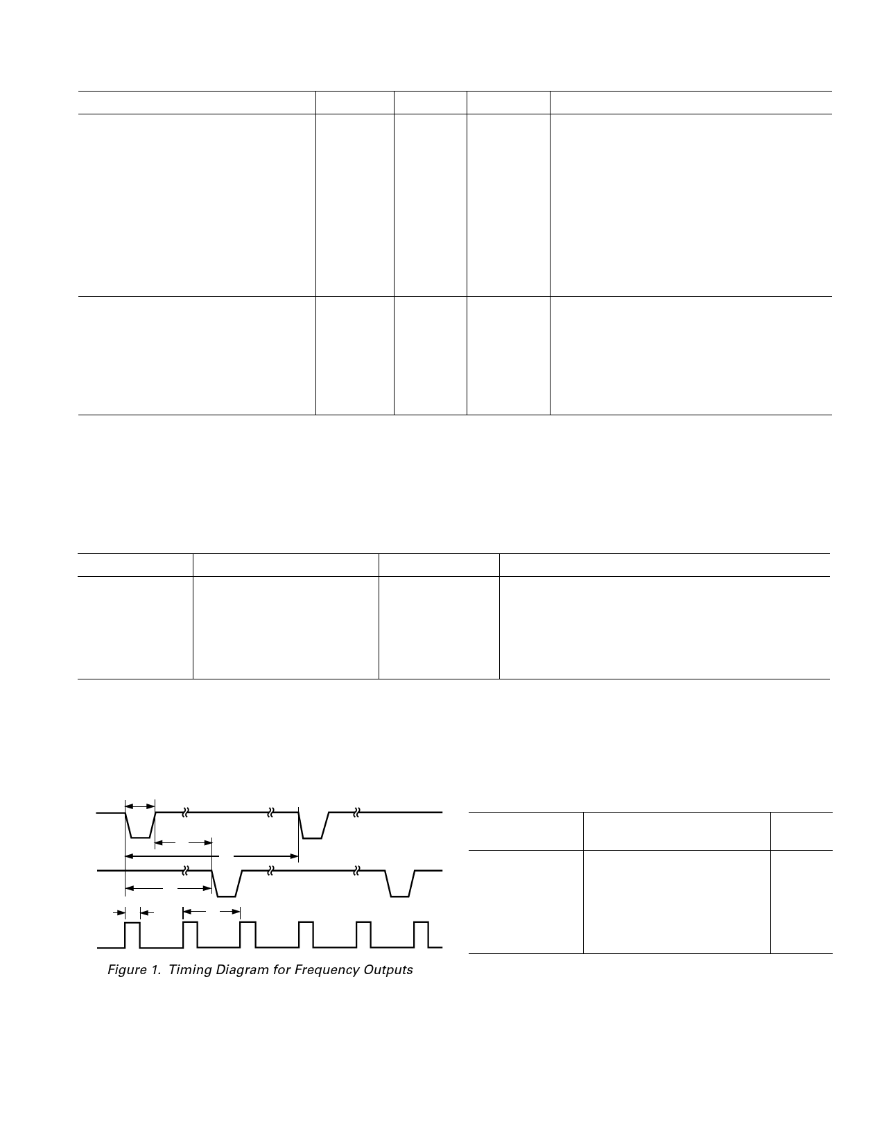
TIMING CHARACTERISTICS1, 2 (AVDD = DVDD = 5 V ؎ 5%, AGND = DGND = 0 V, On-Chip Reference, CLKIN = 3.58 MHz,
TMIN to TMAX = –40؇C to +85؇C)
Parameter
A, B Versions
Unit
Test Conditions/Comments
t13
275
ms
F1 and F2 Pulsewidth (Logic Low)
t2
See Table III
sec
Output Pulse Period. See Transfer Function Section
t3
1/2 t2
sec
Time Between F1 Falling Edge and F2 Falling Edge
t43
90
ms
CF Pulsewidth (Logic High)
t5
See Table IV
sec
CF Pulse Period. See Transfer Function Section
t6
CLKIN/4
sec
Minimum Time Between F1 and F2 Pulse
NOTES
1Sample tested during initial release and after any redesign or process change that may affect this parameter.
2See Figure 1.
3The pulsewidths of F1, F2 and CF are not fixed for higher output frequencies. See Frequency Outputs section.
Specifications subject to change without notice.
t1
F1
.t6
.t2
F2
.t3
t4
.t5
CF
Figure 1. Timing Diagram for Frequency Outputs
ORDERING GUIDE
Model
Package Description
Package
Option
AD7751AAN
AD7751AARS
AD7751ABRS
EVAL-AD7751EB
AD7751AAN-REF
Plastic DIP
Shrink Small Outline Package
Shrink Small Outline Package
AD7751 Evaluation Board
AD7751 Reference Design
PCB (See AN-563)
N-24
RS-24
RS-24
REV. A
–3–
Share Link: 