ADE7757 Ver la hoja de datos (PDF) - Analog Devices
Número de pieza
componentes Descripción
Fabricante
ADE7757 Datasheet PDF : 16 Pages
| |||
ADE7757
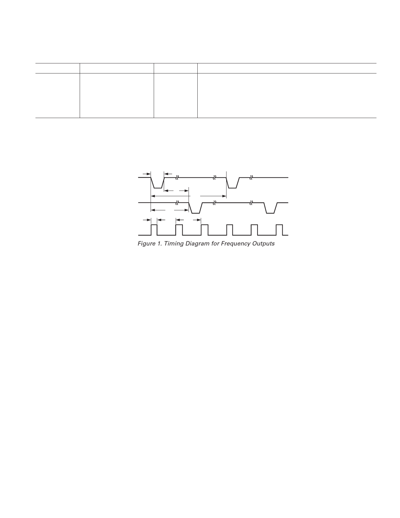
TIMING CHARACTERISTICS1, 2 (VDD = 5 V ؎ 5%, AGND = DGND = 0 V, On-Chip Reference, RCLKIN = 6.2 kΩ,
0.5% ؎ 50 ppm/؇C, TMIN to TMAX = –40؇C to +85؇C, unless otherwise noted.)
Parameter
A, B Versions
Unit
Test Conditions/Comments
t13
244
ms
F1 and F2 Pulse Width (Logic Low).
t2
See Table II
sec
Output Pulse Period. See Transfer Function section.
t3
1/2 t2
t43, 4
173
sec
Time between F1 Falling Edge and F2 Falling Edge.
ms
CF Pulse Width (Logic High).
t5
See Table III
sec
CF Pulse Period. See Transfer Function section.
t6
2
µs
Minimum Time between F1 and F2 Pulses.
NOTES
1Sample tested during initial release and after any redesign or process change that may affect this parameter.
2See Figure 1.
3The pulse widths of F1, F2, and CF are not fixed for higher output frequencies. See Frequency Outputs section.
4The CF pulse is always 35 µs in the high frequency mode. See Frequency Outputs section and Table III.
Specifications subject to change without notice.
t1
F1
t6
t2
F2
t3
t4
t5
CF
Figure 1. Timing Diagram for Frequency Outputs
REV. A
–3–
Share Link: 