ADE7757 Ver la hoja de datos (PDF) - Analog Devices
Número de pieza
componentes Descripción
Fabricante
ADE7757 Datasheet PDF : 16 Pages
| |||
ADE7757
Typical Connection Diagrams
Figure 7 shows a typical connection diagram for Channel V1. A
shunt is the current sensor selected for this example because of
its low cost compared to other current sensors such as the CT
(current transformer). This IC is ideal for low current meters.
SHUNT
RF
؎30mV
V1P
CF
V1N
RF
CF
AGND
PHASE NEUTRAL
Figure 7. Typical Connection for Channel V1
Figure 8 shows a typical connection for Channel V2. Typically,
the ADE7757 is biased around the phase wire, and a resistor
divider is used to provide a voltage signal that is proportional to
the line voltage. Adjusting the ratio of RA, RB, and RF is also a
convenient way of carrying out a gain calibration on a meter.
RA* RB
RF
V2P
CF ؎165mV V2N
RF
CF
NEUTRAL PHASE
*RA >> RB + RF
Figure 8. Typical Connections for Channel V2
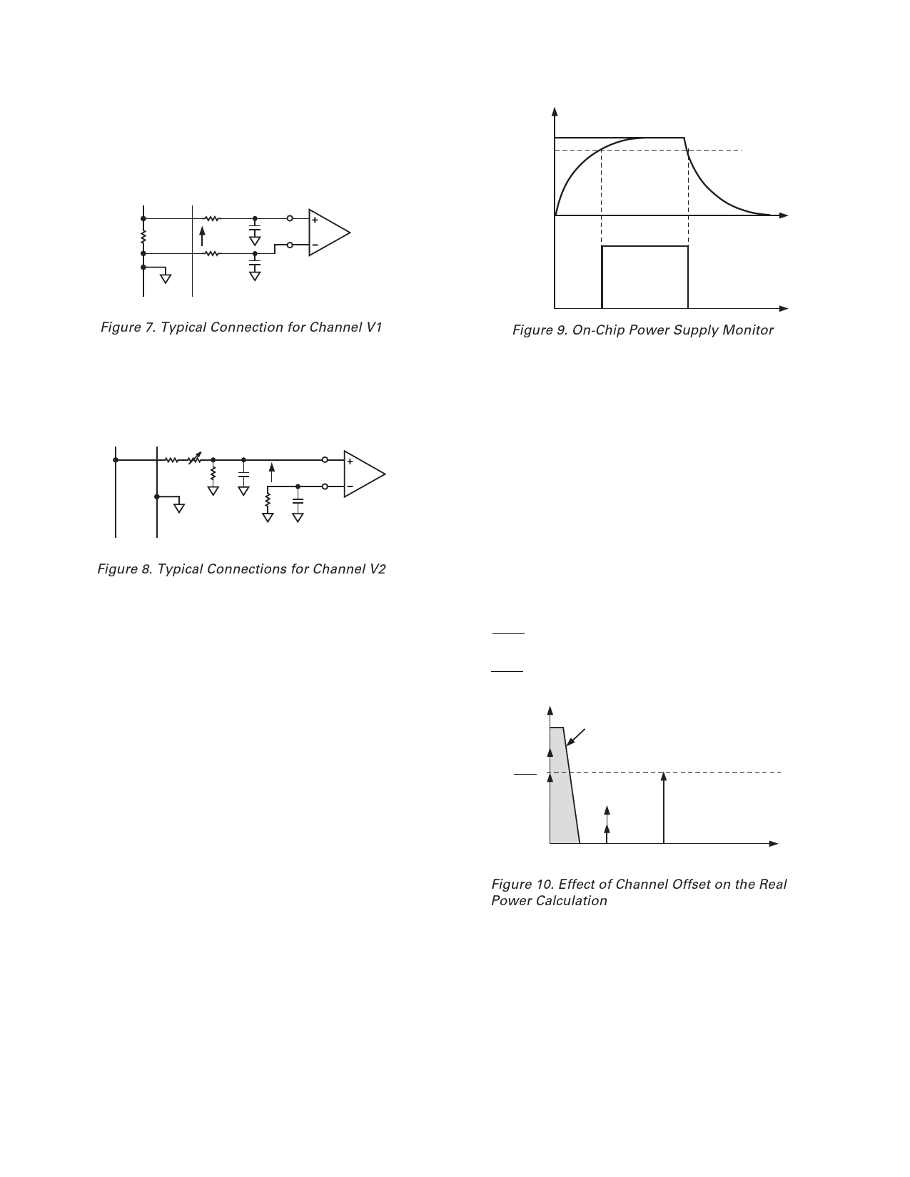
POWER SUPPLY MONITOR
The ADE7757 contains an on-chip power supply monitor. The
power supply (VDD) is continuously monitored by the ADE7757.
If the supply is less than 4 V, the ADE7757 becomes inactive.
This is useful to ensure proper device operation at power-up
and power-down. The power supply monitor has built in hyster-
esis and filtering that provide a high degree of immunity to false
triggering from noisy supplies.
As can be seen from Figure 9, the trigger level is nominally set
at 4 V. The tolerance on this trigger level is within ± 5%. The
power supply and decoupling for the part should be such that
the ripple at VDD does not exceed 5 V ± 5% as specified for
normal operation.
VDD
5V
4V
0V
TIME
INTERNAL
ACTIVATION INACTIVE
ACTIVE
INACTIVE
Figure 9. On-Chip Power Supply Monitor
HPF and Offset Effects
Figure 10 illustrates the effect of offsets on the real power calcu-
lation. As can be seen, offsets on Channel V1 and Channel V2
will contribute a dc component after multiplication. Since this
dc component is extracted by the LPF and used to generate the
real power information, the offsets will contribute a constant
error to the real power calculation. This problem is easily avoided
by the built-in HPF in Channel V1. By removing the offsets
from at least one channel, no error component can be generated
at dc by the multiplication. Error terms at the line frequency ()
are removed by the LPF and the digital-to-frequency conversion
(see Digital-to-Frequency Conversion section).
The equation below shows how the power calculation is affected
by the dc offsets in the current and voltage channels.
{ } { } ( ) ( ) V cos ωt +VOS × I cos ωt + IOS
( ) ( ) = V
×
2
I
+VOS
×
IOS
+VOS
×
I
cos
ωt
+ IOS ×V cos ωt
+V × I × cos(2ωt)
2
VOS ؋ IOS
V؋I
2
DC COMPONENT (INCLUDING ERROR TERM)
IS EXTRACTED BY THE LPF FOR REAL
POWER CALCULATION
IOS ؋ V
VOS ؋ I
0
FREQUENCY – RAD/s
Figure 10. Effect of Channel Offset on the Real
Power Calculation
–10–
REV. A
Share Link: 