AAT1154 Ver la hoja de datos (PDF) - Analog Technology Inc
Número de pieza
componentes Descripción
Fabricante
AAT1154 Datasheet PDF : 16 Pages
| |||
SwitchRegTM
addition, the low pass filter R1 and C3 (shown in Figure
1) filters noise associated with the power switching.
Current Limit and
Over-Temperature Protection
Over-temperature and current limit circuitry protects the
AAT1154 and the external Schottky diode during over-
load, short-circuit, and excessive ambient temperature
conditions. The junction over-temperature threshold is
140°C nominal and has 15°C of hysteresis. Typical
graphs of the over-temperature load current vs. input
voltage and ambient temperature are shown in the
Typical Characteristics section of this document.
Inductor
The output inductor is selected to limit the ripple current
to 20% to 40% of full load current at the maximum input
voltage. Manufacturer’s specifications list both the
inductor DC current rating, which is a thermal limitation,
and the peak current rating, which is determined by the
inductor saturation characteristics. The inductor should
not show any appreciable saturation under normal load
conditions. During overload and short-circuit conditions,
the inductor can exceed its peak current rating without
affecting converter performance. Some inductors may
have sufficient peak and average current ratings yet
result in excessive losses due to a high DC resistance
(DCR). The losses associated with the DCR and its effect
on the total converter efficiency must be considered.
PRODUCT DATASHEET
AAT1154
1MHz 3A Step-Down DC/DC Converter
For a 3A load and the ripple current set to 30% at the
maximum input voltage, the maximum peak-to-peak
ripple current is 0.9A. Assuming a 5V ±5% input voltage
and 30% ripple, the output inductance required is:
L
=
VOUT
IOUT · k ·
FS
·
⎛⎝1 -
VOUT ⎞
VIN(MAX)⎠
=
⎛
⎝
3A
·
3.3V ⎞
0.3 · 1MHz ⎠
·
1
-
⎛ 3.3V ⎞
⎝ 5.25V⎠
= 1.36μH
The factor “k” is the fraction of the full load (30%)
selected for the ripple current at the maximum input
voltage.
The corresponding inductor RMS current is:
IRMS =
⎛
⎝
I
2
O
+
ΔI 2
12
⎞
⎠
≈
IO = 3A
ΔI is the peak-to-peak ripple current which is fixed by
the inductor selection above. For a peak-to-peak current
of 30% of the full load current, the peak current at full
load will be 115% of the full load. The 1.5μH inductor
selected from the Sumida CDRH6D38 series has a 11mΩ
DCR and a 4.0A DC current rating with a height of 4mm.
At full load, the inductor DC loss is 99mW for a 1% loss
in efficiency.
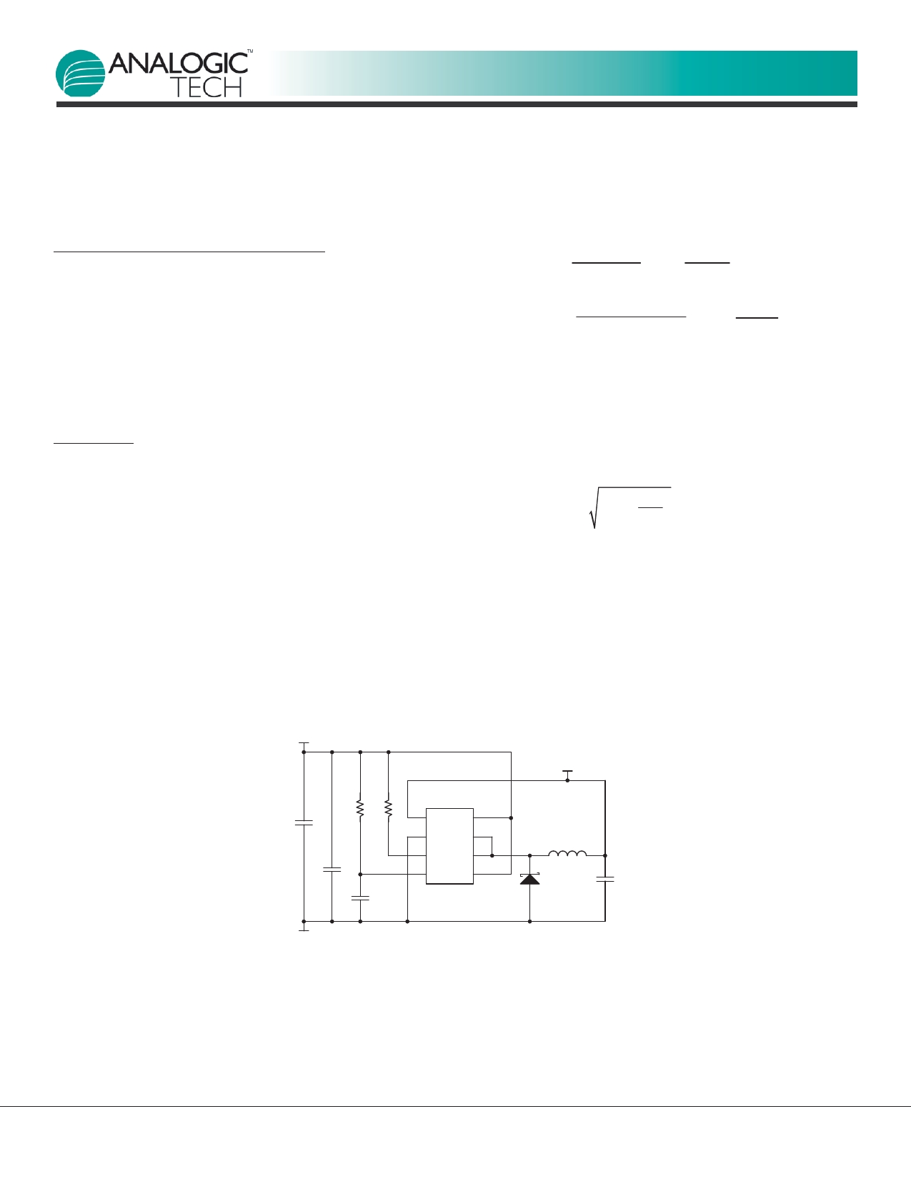
VIN 3.5V to 5.5V
C4
100µF
R1 R2
100 100k
C1
10µF
C3
0.1µF
U1
AAT1154-3.3
FB VP
GND LX
EN LX
VCC VP
VOUT 3.3V @ 3A
L1
1.5µH
D1
C2
B340LA 120µF
+
-
rtn C1 Murata 10µF 6.3V X5R GRM42-6X5R106K6.3
C2 Vishay120µF 6.3V 594D127X96R6R3C2T
C3 0.1µF 0603ZD104M AVX
C4 Vishay Sprague 100µF 16V 595D107X0016C 100µF 16V
D1 B340LA Diodes Inc.
L1 CDRH6D28-1.5µH Sumida
Options
C2 Murata 100µF 6. 3V GRM43-2 X5R 107M 100µF 6.3V (two or three in parallel)
C2 TDK 100µF 6.3V C3325X5R0J107M 100µF 6.3V (two or three in parallel)
Figure 1: 3.3V, 3A Output.
10
www.analogictech.com
1154.2007.11.1.7
Share Link: 