CS51221 Ver la hoja de datos (PDF) - Cherry semiconductor
Número de pieza
componentes Descripción
Fabricante
CS51221 Datasheet PDF : 12 Pages
| |||
TAypppilciaclatPieornfoInrmfoarnmcaetCiohna:rcaocntetrinisutiecds
Design Guidelines
Switch Frequency and Maximum Duty Cycle Calculations
Oscillator timing capacitor, CT, is charged by VREF through
RT and discharged by an internal current source. During
the discharge time, the internal clock signal sets the Gate
output to the low state, thus providing a user selectable
maximum duty cycle clamp. Charge and discharge times
are determined by following general formulas;
( ) tC = RTCTln
(VREF - VVALLEY)
(VREF - VPEAK)
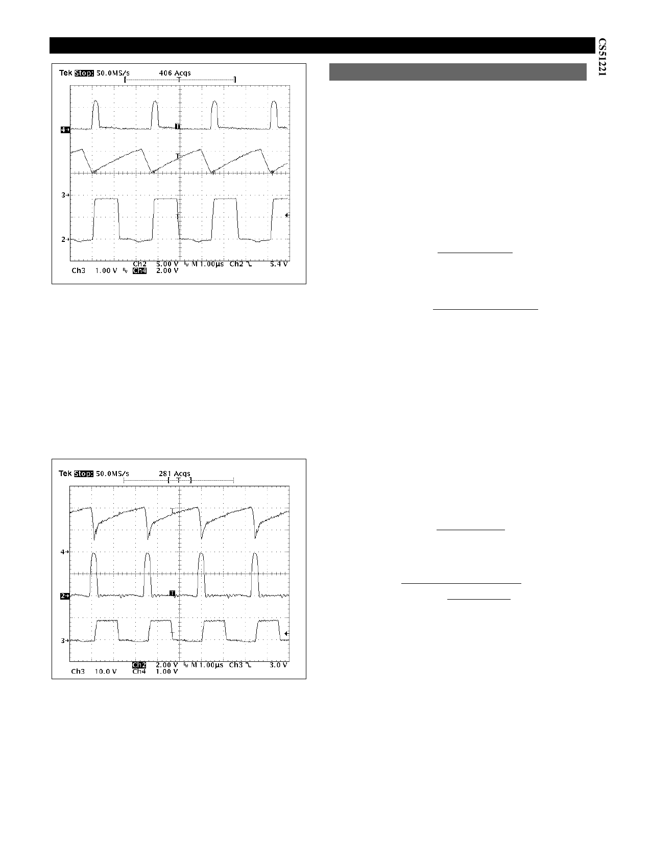
Figure 6: The Sync pin generates a sync pulse at the beginning of each
switching cycle. CH2: GATE Pin, CH3: RTCT, CH4: SYNC pin.
The bi-directional SYNC pin can also receive an external
sync signal of a greater frequency. As show in Fig.7, when
the SYNC pin is triggered by an incoming signal, the IC
immediately discharges CT. The GATE signal is turned on
once the RTCT pin reaches the valley voltage. Because of
the steep falling edge, this valley voltage falls below the
regular 1V threshold. However, the RTCT pin voltage is
then quickly raised by a clamp. When the RTCT pin reaches
the 0.95V(typ) Valley Clamp Voltage, the clamp is discon-
nected after a brief delay and CT is charged through RT.
( ) td = RTCTln
(VREF - VPEAK - IdRT)
(VREF - VVALLEY - IdRT)
,
where
tC = charging time;
td = discharging time;
VVALLEY = valley voltage of the oscillator;
VPEAK = peak voltage of the oscillator.
Substituting in typical values for the parameters in the
above formulas:
VREF = 3.3V, VVALLEY = 1V, VPEAK = 2V, Id = 1mA
tC = 0.57RTCT
( ) td = RTCTln
1.3 - 0.001RT
2.3- 0.001RT
0.57
( ) Dmax =
0.57+ In
1.3 - 0.001RT
2.3- 0.001RT
It is noticed from the equation that for the oscillator to
function properly, RT has to be greater than 2.3k.
Figure 7: Operation with external sync. CH 2: SYNC pin, CH3: Gate pin,
G4: RTCT pin.
9
Share Link: 