CS51221 Ver la hoja de datos (PDF) - Cherry semiconductor
Número de pieza
componentes Descripción
Fabricante
CS51221 Datasheet PDF : 12 Pages
| |||
PACKAGE PIN #
16L PDIP & 16L SO Narrow
1
2
3
4
5
6
7
8
9
10
11
12
13
14
15
16
TypicaPl aPcekrafogremPainncDe eCshcrairpatcitoenristics
PIN SYMBOL
FUNCTION
GATE
ISENSE
SYNC
FF
UV
OV
RT/CT
ISET
VFB
COMP
SS
LGnd
VREF
VCC
PGnd
VC
External power switch driver with 1.0A peak capability. Rail to
rail output occurs when the capacitive load is between 470pF
and 10nF.
Current sense comparator input.
Bidirectional synchronization. Locks to highest frequency.
PWM ramp.
Undervoltage protection monitor.
Overvoltage protection monitor.
Timing resistor RT and capacitor CT determine oscillator
frequency and maximum duty cycle, DMAX.
Voltage at this pin sets pulse-by-pulse overcurrent threshold.
Feedback voltage input. Connected to the error amplifier
inverting input.
Error amplifier output.
Charging external capacitor restricts error amplifier output
voltage during the power up or fault conditions.
Logic Ground.
3.3V reference voltage output. Decoupling capacitor can be
selected from 0.01µF to 10µF.
Logic supply voltage.
Output power stage ground.
Output power stage supply voltage.
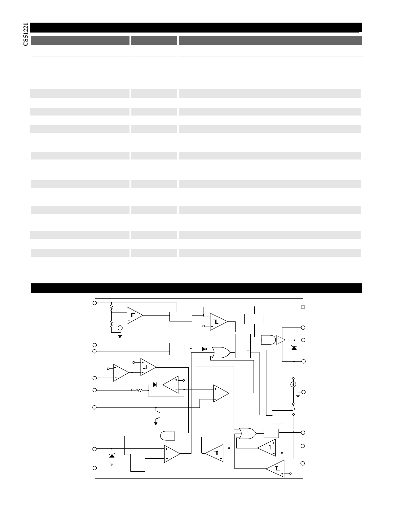
Block Diagram
VCC
SYNC
RTCT
VFB
UVL
+
-
UV Lockout
Start/Stop
ENABLE VREF = 3.3V
3.3V
3.1V
VREF OK
S
3.0V
VBG
(1.263V) EAMP
2V to 1V Trip Points
OSC
Max Duty Cycle
(Sat Sense)
SS to 1.8V Max
G2
R
COMP
Soft Start Clamp
PWM
Comp
Thermal
Shutdown
2mA(maximum load current) VREF
Low
VC
Sat
Gate
Q
Driver
G1
GATE
Q
13.5V
PGnd
VREF
50µA
LGnd
FF
ISET
ISENSE
DISABLE 150ns
Blank
FF Discharge
G3
ILIM
ON
Max SS
Det
3.0V
(Sat Sense)
VO Off
G4
Latching
Discharge 5µA
SS
OV Monitor
OV
2V
UV Monitor
UV
1V
6
Share Link: 